
A 2.2 to 2.4 GHz Dual 8 x 2 Switch Matrix
Technical Research and Manufacturing Inc. (TRM)
Bedford, NH
One of the key components of a phased-array radar system is the RF switching network that directs the various RF signals to and from the respective antenna elements. This switching matrix must be both phase and amplitude balanced to assure proper operation and provide a low loss path with good isolation.
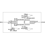
The model SW-16423 dual 8 x 2 switch matrix was designed to fulfill these needs, acting as the main building block for a much larger matrix in a mobile phased-array radar system. The unit is an SMA-connectorized assembly 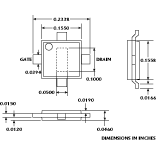 featuring a two-way power divider at each input port. The output of each divider leg feeds a GaAs SPST matched switch. In turn, the output of each switch feeds the input of a two-way combiner whose output is fed to the input of a four-way combiner. Ultimately, the output of this four-way combiner becomes one of the four matrix outputs. Figure 1 shows the block diagram for one of the 8 x 2 switch matrices in the dual assembly.
The printed microstrip construction utilized in the design of the switch matrix results in a ± 2° phase balance specification over the 2200 to 2400 MHz frequency range. This level of phase balance is very important in phased-array or other beamforming applications.
Another important feature of the switch matrix is the use of GaAs FET switches. The incorporation of GaAs technology reduces current consumption dramatically over conventional PIN diode devices. In addition, the use of GaAs technology also allows the switch assembly to operate from positive bias only, reducing the final assembly wiring and circuit complexity. The entire assembly operates from a +10 V DC supply and draws 150 mA.
 The twin eight-input switch banks, each of which provides dual-output ports, are controlled through a nine-pin D connector allowing full-access, single-line TTL control for each input. The RF input power is specified at 0 dBm. The switch assembly offers 16 dB maximum insertion loss with +/-0.5 dB amplitude balance. Figure 2 shows the switch matrix’s phase
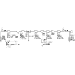 balance, and insertion loss and amplitude balance. SWR for all input and output ports is specified at 1.45 maximum (–14.7 dB return loss) with isolation between inputs specified at 30 dB minimum, as shown in Figure 3 . Switching speed was designed to
  be a modest 2 ms maximum, however, the performance of the GaAs switches far exceeds this requirement, providing a typical transition time in a range below 100 ns.
The model SW-16423 8 x 2 dual-switch matrix is supplied in a 16.16" x 6.00" x 0.88" housing (excluding SMA-M input and SMA-F output connectors and the D connector). Multiple combinations of the switch matrix can be used to create a much larger matrix similar to the assembly shown in Figure 4 .
Technical Research and Manufacturing Inc. (TRM),
Bedford, NH
(603) 627-6000.