
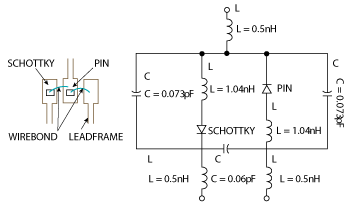
Figure 1 SOT-323 packaged PIN-Schottky diode pair (left) and package equivalent circuit model.
The Schottky-PIN limiter provides better receiver protection than a PIN diode-only limiter because it has a ~10 dB lower limiting threshold; however, its insertion loss has a strong impact on the overall noise figure because it typically precedes the gain stages. The extra diode in the Schottky-PIN limiter results in higher loss than the PIN diode-only limiter. The main loss contributors are the diodes’ parasitic capacitances, which load the signal path. In addition, the use of low cost, plastic packaged diodes introduces substantially more loss than either bare chips or hermetically packaged diodes.
Aside from reducing diode parasitic capacitance by either stacking1 or mesa construction,2 limiter loss can be minimized using circuit techniques. The loading effect of the Schottky diode on the RF path can be reduced with either a high-impedance, quarter wavelength line3 or a directional coupler,4,5 but these passive components add to either the size or cost, and furthermore, they detrimentally increase the limiting threshold. A new design recently demonstrated that a PIN-Schottky limiter’s insertion loss can be improved by integrating the two discrete diodes’ parasitic capacitances into a lowpass ladder network.6 The ladder configuration preserves the low limiting threshold, but requires that the PIN diode have two anode connections.
Traditionally, the PIN-Schottky limiter is fabricated using separate diodes, but we recently combined two diodes in a SOT-323 package to achieve greater miniaturization7 and demonstrated its viability in a microwave limiter application.8 The three-pin package, however, limits the PIN diode to one anode connection (see Figure 1). To reduce the insertion loss of microwave limiters fabricated with this device, a lowpass Π configuration for absorbing the parasitic capacitances was devised. This article summarizes resulting performance improvements using the lowpass Π configuration in a 1.8 GHz limiter.
Hybrid Limiter with PIN and Schottky Diodes
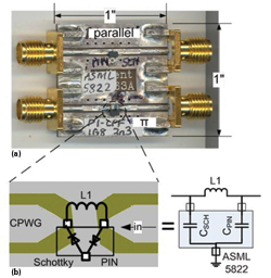
Figure 2 Test fixture for evaluating the PIN-Schottky diode pair (a); External inductor (L1) forms a Π lowpass network with diodes' parasitic capacitances (b).
The PIN diode, which forms the signal-attenuating half of the limiter component, can be functionally described by its 1.5 µm I-layer and a 100 µm diameter.9 The first dimension determines the limiter’s turn-on threshold,10 transient response time11 and spike leakage;12,13 whereas, the second dimension caps its power dissipation. The APLAC simulation parameters (see Table 1) complete the PIN diode description. The Schottky diode, which constitutes the signal detecting half of the limiter component, can be described by a 250 mV barrier height at 1 mA14,15 and a set of SPICE parameters (see Table 2).
Electrical connections between the diode chips and the package leads are made using a combination of conductive epoxy and bond-wires (see Figure 1). A low thermal resistance of 150°C/W, achieved by attaching the diode chips directly to the copper lead-frame, improves power dissipation. The package leads and bondwires contribute ~0.5 and ~1 nH, respectively, to the component’s equivalent circuit model. The plastic encapsulation adds ~73 fF parasitic capacitances across the diodes. Measured at the package terminals, the PIN and Schottky diodes’ zero bias capacitances at 1 MHz are ~0.9 and ~0.7 pF, respectively. When the two diodes are connected in parallel in the limiter circuit, they present a combined ~1.6 pF capacitance in shunt with the RF path.
Evaluation Fixture
The evaluation fixture consists of a 30 mil thick FR-4 PCB containing two 50 Ω co-planar waveguide (CPWG) with ground transmission lines (see Figure 2). The first line is continuous, but the second line has a narrow gap in the middle. The PIN-Schottky diode pair mounted on the continuous line acts as an experimental control; the circuit arrangement, two diodes connected in parallel, is the one originally envisaged for this component. The second PIN-Schottky diode pair is mounted on the gapped line with its adjacent leads straddling the gap. The diodes’ capacitances form the shunt arms of a lowpass Α network. A chip inductor L1, which bridges the same gap, forms the series arm. Following the norm for this class of limiter, the PIN diode side is defined as the signal input.
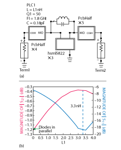
Figure 3 Simulation shows lower loss for the π configuration at 1.8 GHz (a); simulated results (b).
Simulation
Through simulation, L1 is optimized for minimum loss at the operating frequency. To model the PIN-Schottky diode pair, APLAC and SPICE parameters from Tables 1 and 2 are combined inside the symbol X3 in Figure 3a. The frequency of 1.8 GHz is chosen for evaluation because it is the device’s upper limit. Figure 3b shows that an inductance of 3.2 nH results in the lowest insertion loss (~0.4 dB), while the best return loss occurs at a slightly higher inductance of 3.4 nH. The physical realization uses a standard value of 3.3 nH from the Toko LL1608 series.
The limiter circuit containing the paralleled diodes is represented by the condition L1 = 0. A higher loss of 1.2 dB is obtained with the diodes mounted in parallel following the datasheet’s recommendations. The results include an estimated fixture loss of 0.25 dB.
Experimental Results
Experimental results confirm improved performance of the Π configuration over the parallel connection (see Figure 4). After 0.25 dB of fixture loss is removed from the raw data, a 0.9 dB difference is recorded between the two configurations at 1.8 GHz. Despite optimization at 1.8 GHz, improvement is maintained over a 1 GHz bandwidth.
The Π configuration can be optimized for reduced loss at other frequencies via L1, however, in addition to increasing insertion loss with frequency, isolation also degrades. Isolation degrades with frequency due to parasitic inductance in series with the PIN diode. This particular Schottky-PIN pair has ~2 nH of parasitic series inductance (see Figure 1). This limits its isolation to approximately 8 to 10 dB at 1.8 GHz. Components with lower parasitic inductance should produce better performance at higher frequencies.
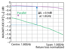
Figure 4 New configuration reduces 1.8 GHz insertion loss by 0.9 dB.
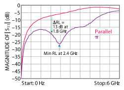
Figure 5 New configuration increases 1.8 GHz return loss by 13 dB.
The Π-configured limiter is also significantly less reflective than the parallel-connected ‘control’ (see Figure 5). At 1.8 GHz, the π configuration achieves ~13 dB lower return loss than the control. The largest improvement occurs at ~2.4 GHz or ~33 percent higher than the design frequency, although we are not able to explain the responsible mechanism.
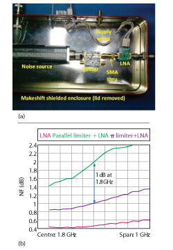
Figure 6 Cascaded Π limiter/LNA NF reduces NF by 1 dB versus parallel limiter/LNA; physical circuit (a), measured performance (b).
The measured noise figure of a cascaded limiter and low noise amplifier (LNA) confirms the Π configuration’s lower loss. The test setup replicates the configuration of a limiter to protect an LNA input. The 1.8 GHz LNA uses a MGA-634P8 GaAs ePHEMT MMIC16 and has a ~ 0.5 dB NF at its connectors.17 The first combination of Π limiter and LNA achieves ~1 dB NF, whereas, the second combination consisting of a parallel limiter and the LNA is significantly noisier at ~2 dB NF (see Figure 6). The difference between the two can be predicted from the limiters’ insertion loss. In a final product, the cascaded NF should be < 0.8 dB because the limiter fixture and the SMA ‘through’ adapter add ~0.25 dB loss to the experimental results.
The Π configuration also outperforms the alternative loss mitigating scheme based on the ladder network.6 To ensure a fair comparison, the ladder-configured limiter is fabricated from the same PIN and Schottky diode chips as the Π limiter, but the former’s diodes are assembled into separate SOT-323 packages so that its PIN diode can have the required dual anodes. At 1.8 GHz, the Π configuration has ~0.2 dB insertion loss versus the ladder configuration’s ~0.4 dB (see Figure 7). Besides providing lower loss, the Π configuration occupies approximately half the PCB space of the ladder configuration.
Conclusion
A 1.8 GHz limiter based on a three-pin hybrid Schottky-PIN diode component can benefit from lower loss and better matching when the diodes’ parasitic capacitances are configured into a Π network, as compared to the manufacturer recommended parallel diode connection. Although demonstrated with an ASML-5822 PIN-Schottky diode pair, the proposed configuration has general utility. Since most packaged PIN diodes are available only in single-anode styles, (e.g. SOD-323, SOD-523, beam lead and glass diodes) and two anodes are required in the competing ladder configuration, the π configuration expands the number of usable devices. Moreover, the Π configuration achieves lower loss than the ladder configuration when fabricated with a similar set of PIN and Schottky diode chips. Future work will investigate large-signal (limiting) and transient performance of the Π configuration.
Acknowledgment
The author thanks L.L. Vong measuring the package parasitics, R.W. Waugh for designing the PCB, and, S.A. Asrul and the management of Avago Technologies for approving the publication of this work.
References
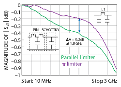
Figure 7 Π Limiter exhibits 0.2 dB lower insertion loss than the ladder limiter at 1.8 GHz.
- D.G. Smith, D.D. Heston and D.L. Allen, “Designing High-Power Limiter Circuits With GaAs PIN Diodes,” IEEE International Microwave Symposium Digest, Vol. 1, June 1999, pp. 329-332.
- Alpha Application Note 80300, “Characteristics of Semiconductor Limiter Diodes,” Specifications, Application Notes, Packages, Alpha Industries Inc., Semiconductor Division, 1985, pp. 3-45.
- L.G. Maloratsky, “Transceiver Duplexer Design Considerations,” Microwave Journal, Vol. 51, No. 10, October 2008, pp. 68-86.
- B.M. Coaker and D.M. Dowthwaite, “Planar Limiters and Receiver Protectors,” Proceedings of the 4th European Radar Conference, October 2007, pp. 405-408.
- Skyworks Application Note APN1018, “PIN Limiter Diodes in Receiver Protectors,” available at: www.skyworksinc.com.
- C.L. Lim, “Reduce Losses in RF Schottky-PIN Limiters Circuits,” Electronic Design, October 2012, available at: electronicdesign.com/article/communications/reduce-losses-rf-schottkypin-limiter-circuits-74519.
- Avago Technologies Product Specification, “ASML-5822 Low Power Limiter Diode,” available at: www.avagotech.com.
- C.L. Lim, “Wideband Limiter Fits SOT-323 Pack,” Microwaves & RF, July 2010, pp. 75-83.
- Avago Technologies Datasheet, “Surface Mount RF PIN Switch and Limiter Diodes – HSMP-382x and HSMP-482x series,” available at: www.avagotech.com.
- Avago Technologies Application Note 1050, “Low Cost Surface Mount Power Limiters,” available at: www.avagotech.com.
- R.J. Tan, A.L. Ward and R. Kaul, “Transient Response of PIN Limiter Diodes,” IEEE International Microwave Symposium Digest, Vol. 3, June 1989, pp. 1303-1306.
- R.J. Tan, A.L. Ward, R.V. Garver and H. Brisker, “PIN Diode Limiter Spike Leakage, Recovery Time and Damage,” IEEE International Microwave Symposium Digest, Vol. 1, May 1988, pp. 275-278.
- A.L. Ward, R.J. Tan and R. Kaul, “Spike Leakage of Thin Si PIN limiters,” IEEE Transactions on Microwave Theory and Techniques, Vol. 42, No. 10, October 1994, pp. 1879-1885.
- Avago Technologies Product Specification, “HSMS-282x series,” available at: www.avagotech.com.
- R.W. Waugh, “A Schottky Diode Optimized for Consistency,” Agilent Technologies Design Tip, available at: www.hp.woodshot.com/hprfhelp/5_downld/lit/diodelit/dt_d002.pdf.
- Avago Technologies Datasheet, “MGA-634P8 Ultra Low Noise, High Linearity Low Noise Amplifier,” available at: www.avagotech.com.
- Avago Technologies Application Note 5475, “MGA-634P8 GaAs ePHEMT MMIC 1900 MHz Low Noise Amplifier With Superior Noise and Linearity Performance,” available at: www.avagotech.com.