
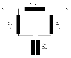
Figure 1 Lowpass filter structure.
A compact, wide stopband lowpass filter using a tri-section impedance hairpin resonator with three transmission zeros is described. Measured results demonstrate a sharp transition rate from transmission to cutoff of 61.8 dB/GHz and a wide stopband of 1.06 to 5.3 GHz with out-of-band rejection higher than 20 dB.
Compact sized microwave lowpass filters (LPF) with wide stopbands and sharp cutoff frequencies are needed in various wireless communication systems to suppress harmonics and spurious signals; however, conventional LPFs, using open-circuited stubs and stepped impedances, are large and have narrow stopbands with a gradual cutoff.1 To improve performance, the usual approach is to raise the order of the stepped impedance, making the circuit larger without significantly improving the cutoff skirt. LPFs using defected ground structures (DGS)2-6 and coupled-line structures7-11 have been recently proposed. The LPF with DGS proposed by Ahn et al2 and the coupled line LPF with three attenuation poles described by Lee et al7 both have very gradual cutoff skirts. The filter described by Hsieh and Chang12 also suffers from this problem because the only transmission zero in the stopband is far from the cutoff frequency. For the DGS resonator described by Chen and Xu,5 two transmission zeros are applied to the LPF, which has a sharp rejection slope and a very wide stopband; however, this design is complex and has fabrication difficulties. In Veledi et al9 and Wei et al,10 both LPFs using coupled-line hairpin units have wide stopbands, but rejection is very poor at some frequencies.
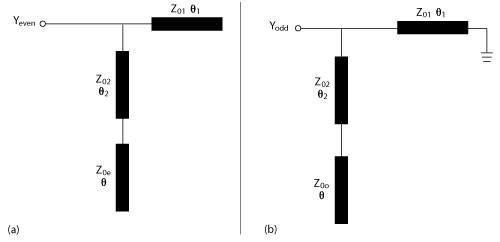
Figure 2 Equivalent circuit. Even-mode (a). Odd-mode (b).
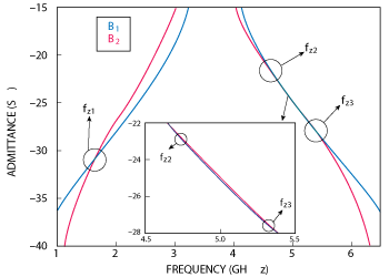
Figure 3 The curves of B1 and B2 (Z01 = 160 Ω, Z02 = 40 Ω, Z0e = 35 Ω, Z0o = 23 Ω, θ = 22.2° at 1 GHz, θ1 = 24.5° at 1 GHz, θ2 = 2° at 1 GHz).
To address these deficiencies, we describe a structure with three transmission zeros in the stopband using a tri-section impedance hairpin resonator. This structure is compact and has a wide stopband and a sharp cut-off frequency response.
THEORETICAL ANALYSIS
Figure 1 shows the structure of the proposed lowpass filter. The feed lines are linked to the joining ends of transmission lines whose characteristic impedances and electrical lengths are Z01, Z02 and θ1, θ2, respectively. The coupled line, which has even- and odd-mode impedances Z0e and Z0o and electrical length θ, is connected to the remaining ends of the two symmetrical transmission lines with characteristic impedance Z02. Because the structure is symmetrical, it can be analyzed by using odd- and even-mode networks.
When the structure is excited by the even mode, the equivalent circuit is depicted in Figure 2a. The even-mode admittance of the circuit is
When the structure is excited by the odd-mode, the corresponding equivalent circuit is shown in Figure 2b. The odd-mode admittance of the circuit is
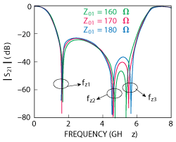
Figure 4 |S21| of the structure with different characteristic impedances (Z01). (Z02 = 40 Ω, Z0e = 35 Ω, Z0o = 23 Ω, θ = 22.2° at 1 GHz, θ1 = 24.5° at 1 GHz, θ2 = 2° at 1 GHz).
The transmission coefficient of the total network is obtained by
where Y0 is the characteristic admittance of the input and output transmission lines.
When |S21|=0, the transmission zeros meet the following requirement:

where
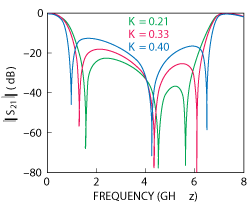
Figure 5 |S21| of the structure with different coupling factors (K). (Z1 = 180 Ω, Z2 = 40 Ω, θ = 22.2° at 1 GHz, θ1 = 24.5° at 1 GHz, θ2 = 2° at 1 GHz).
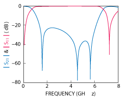
Figure 6 |S11| and |S21| of the structure. (Z1 = 180 Ω, Z2 = 40 Ω, Z0e = 35 Ω, Z0o = 23 Ω, θ =22.2° at 1 GHz, θ1 = 24.5° at 1 GHz, θ2 = 2° at 1 GHz).
As shown in Figure 3, the curves of reactance B1 and B2 have three common points, which means that Equation 4 has three answers. The locations of the three points in Figure 4 (Z01=160 ohms) are nearly the same as these three transmission zeros. When increasing the characteristic impedance Z01, the position of the first zero (fz1) is almost the same, while the distance between fz2 and fz3 becomes longer. In fact, the locations of fz2 and fz3 both change slightly and, the rejection between these two frequencies decreases with increasing Z01. Z01 should be chosen to achieve the desired stopband rejection based on the analysis and observations.
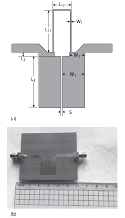
Figure 7 Layout (a) and photograph (b) of the test circuit.
Frequency responseis also affected by the coupled line. The coupling factor is defined as K = (Z0e- Z0o) / (Z0e+ Z0o). As shown in Figure 5, the first transmission zero (fz1) moves to the lower side with an increase in K, resulting in a sharper cutoff frequency and a smaller circuit size. The second zero (fz2) moves to the lower side while the third zero (fz3) moves to the higher side, increasing the distance between fz1 and fz2 and between fz2 and fz3. This provides a broader stopband, but with decreased rejection between the transmission zeros, especially between fz2 and fz3.
Analysis of the final design predicts very good performance (see Figure 6). The 20 dB stopband width is very broad, ranging from almost 1 to 6 GHz and rejection is high. In addition, the cutoff skirt is sharp, improving the lowpass response.
FABRICATION AND MEASUREMENT
An LPF was fabricated on a substrate with a thickness of 1.5 mm and relative dielectric constant of 2.65 (see Figure 7). The circuit dimensions are: w1 = 0.15 mm, l11= 15.6 mm, l12 = 5.56 mm, w2 = 5.5 mm, l2 = 1.5 mm, w3 = 8 mm, l3 = 16.5 mm and s = 0.16 mm. The overall circuit size is 34 × 16 mm(0.08λg × 0.04λg, where λg is the guide wavelength at fc). The filter’s size is much smaller than the sizes in references 13-15, which is very compact so as to meet the requirement of miniaturization.
Simulations with Agilent Technologies’ Advanced Design System (ADS) agree closely with measurements using an Agilent 8510C vector network analyzer (see Figure 8). The measured 3 dB passband extends from DC to 0.54 GHz. Three transmission zeros are located at 1.3 GHz with S21 = -50 dB, at 3.57 GHz with S21 = -56.6 dB and at 5.22 GHz with S21 = -26 dB. Rejection is greater than 20 dB from 1.06 to 5.3 GHz (a fractional bandwidth of 133 percent). The roll-off rate is 61.8 dB/GHz (attenuation: 3 dB at 0.54 GHz and 50 dB at 1.3 GHz).
CONCLUSION
A compact lowpass filter with three transmission zeros using a tri-section impedance hairpin resonator is described. By tuning the transmission line parameters, three zeros are used to expand the stopband, sharpen the cutoff frequency and deepen the rejection. The measured results agree with the simulations and show that this filter has very attractive features: sharp transition, a very compact circuit size and a wide stopband.
ACKNOWLEDGMENTS
This work has been supported by the National Natural Science Foundation of China under grants (61101052, 60873020, and 61070063), Zhejiang Provincial Natural Science Foundation under grants (Y1110297, Z1080702) and the Foundation of Zhejiang Sci-Tech University under grants (1004811-Y).
References
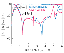
Figure 8 Measurement versus simulation.
- J.S. Hong and M.J. Lancaster, Microstrip Filters for RF/Microwave Applications, New York, Wiley, 2001.
- D. Ahn, J.S. Park, C.S. Kim, J. Kim, Y. Qian and T. Itoh, “A Design of the Low-Pass Filter Using the Novel Microstrip Defected Ground Structure,” IEEE Transactions on Microwave Theory and Techniques, Vol. 49, No. 1, January 2001, pp. 86-93.
- R.Y. Sharma, T. Chakravarty, S. Bhooshan and A.B. Bhattacharyya, “Design of a Novel 3 dB Microstrip Backward Wave Coupler Using Defected Ground Structure,” Progress in Electromagnetics Research, Vol. 65, 2006, pp. 261-273.
- X.Q. Chen, R. Li, S.J. Shi, Q. Wang, L. Xu and X.W. Shi, “A Novel Low Pass Filter Using Elliptic Shape Defected Ground Structure,” Progress in Electromagnetics Research B, Vol. 9, 2008, pp. 117-126.
- Q. Chen and J. Xu, “DGS Resonator With Two Transmission Zeros and its Application to Lowpass Filter Design,” Electronics Letters, Vol. 46, No. 21, October 2010, pp. 1447-1449.
- J. Chen, Z.B. Weng, Y.C. Jiao and F.S. Zhang, “Lowpass Filter Design of Hilbert Curve Ring Defected Ground Structure,” Progress In Electromagnetics Research, Vol. 70, 2007, pp. 269–280.
- Y.W. Lee, S.M. Cho, G.Y. Kim, J.S. Park, D. Ahn and J.B. Lim, “A Design of the Harmonic Rejection Coupled Line Low-Pass Filter With Attenuation Poles,” Asia-Pacific Microwave Conference Proceedings, Vol. 3, November 1999, pp. 682-685.
- Y. Wu, Y. Liu, S. Li and C. Yu, “A New Wide-Stopband Low-Pass Filter with Generalized Coupled-Line Circuit and Analytical Theory,” Progress In Electromagnetics Research, Vol. 116, 2011, pp. 553-567.
- V. K. Velidi and S. Sanyal, “Sharp Roll-Off Lowpass Filter With Wide Stopband Using Stub-Loaded Coupled-Line Hairpin Unit,” IEEE Microwave and Wireless Components Letters, Vol. 21, No. 6, June 2011, pp. 301-303.
- F. Wei, L. Chen, X.W. Shi, Q.L. Huang and X.H. Wang, “Compact Lowpass Filter With Wide Stop-Band Using Coupled-Line Hairpin Unit,” Electronics Letters, Vol. 46, No. 1, January, 2010, pp. 88-90.
- S. Luo, L. Zhu and S. Sun, “Stopband-Expanded Low-Pass Filters Using Microstrip Coupled-Line Hairpin Units,” IEEE Microwave and Wireless Components Letters, Vol. 18, No. 8, August 2008, pp. 506-508.
- L.H. Hsieh and K. Chang, “Compact Elliptic-Function Low-Pass Filters Using Microstrip Stepped-Impedance Hairpin Resonators,” IEEE Transactions on Microwave Theory and Techniques,Vol. 51, No. 1, January 2003, pp. 193-199.
- R. Li, D. Kim and C.M. Choi, “Compact Structure With Three Attenuation Poles for Improving Stopband Characteristics,” IEEE Microwave and Wireless Components Letters, Vol. 16, No. 12, December 2006, pp. 663-665.
- L. Li, Z.F. Li and J.F. Mao, “Compact Lowpass Filters With Sharp and Expanded Stopband Using Stepped Impedance Hairpin Units,” IEEE Microwave and Wireless Components Letters, Vol. 20, No. 6, June 2010, pp. 310-312.
- W.H. Tu and K. Chang, “Compact Microstrip Low-Pass Filter With Sharp Rejection,” IEEE Microwave and Wireless Components Letters, Vol. 15, No. 6, June 2005, pp. 404-406.