
A sharp-rejection wideband bandstop filter (WBSF) is designed in a compact, planar form factor. Three transmission zeros are excited to create a wide stopband response that is easily adjusted by tuning the physical parameters of the structure. The assembled filter demonstrates an 89.5 percent stopband with a rejection of more than 50 dB at both transitions. The circuit area is 0.022λg.2
he WBSF is a key enabler for suppressing unwanted signals in broadband wireless systems. Conventional microstrip BSFs1 consisting of shunt open-circuited stubs are relatively large and have narrow stopbands. Today, however, various methods and structures are available to increase filter rejection in a reduced size. Qian2 introduces a new compact WBSF with a multilayer embedded capacitor in LTCC. It has a wide bandwidth, but has low rejection levels. Mandal and Sanyal3 describe a structure consisting of two parallel coupled microstrip line sections in shunt connection, while Shaman and Hong4 use a cross-coupled configuration. For both of these filters, rejection decreases with wider bandwidth and their 20 dB fractional bandwidths are narrower than desired. To address this, a filter designed with a coupled line and two signal paths, is proposed by Sánchez-Soriano and Torregrosa-Penalva,5 however, its size can still be decreased. High rejection is achieved by Chiou and Tai6 with a dual-band BSF using a dual-mode loop resonator and a cross-coupled capacitor. Its 20 dB FBW is over 100 percent, but the exact capacitance is hard to control at high frequencies.
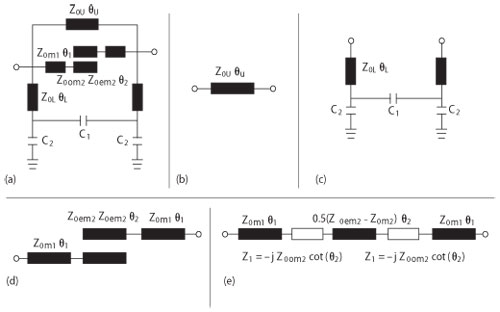
Figure 1 BSF equivalent circuit model with coupling structure (a); upper section (b); lower section (c); middle section (d); equivalent circuit (e).
This article describes a new compact WBSF topology in planar microstrip with three transmission zeros in the stopband (see Figure 1). Design equations and parametric curves are provided. The WBSF not only improves rejection and bandwidth, but is also compact and is easy to design, control and fabricate.
Analysis
Figure 1a is the equivalent circuit model of the bandstop filter (BSF). It can be regarded as an electrical network composed of three parallel parts shown in Figure 1b, c and d, respectively. Figure 1b, the upper section of the BSF, is a transmission line having a characteristic impedance (Z0U) and electrical length (θU). The lower section, Figure 1c, is composed of a pi network model consisting of three capacitors C1 and C2, and two bilateral transmission lines with characteristic impedance (Z0L) and electrical length (θL). The middle section, Figure 1d, consists of a parallel-coupled line with two extended transmission lines. Both extended transmission lines have the same characteristic impedance (Z0m1) and electrical length (θ1). The parallel-coupled transmission line between them has an odd-mode impedance (Z0om2), an even-mode impedance (Z0em2) and electrical length (θ2). It is made equal to the structure composed of reactance (Z1) and a transmission line with impedance 0.5(Z0em2-Z0om2) and electrical length 0.5θ2. The transformed equivalent circuit is shown in Figure 1e.
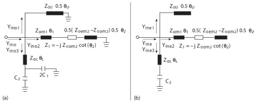
Figure 2 Equivalent circuit; even-mode (a), odd mode (b).
Since the configurations in Figures 1b, c and e are all symmetrical, they can be decomposed into even- and odd-mode excitations, as shown in Figure 2.
When excited in the odd-mode, its input admittance is given by
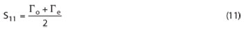
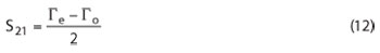
and the input reflection is
where Z0 is the port impedance.
Similarly, when the circuit is excited in the even-mode, the input admittance is given by
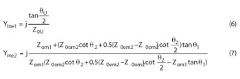
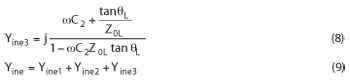
and the input reflection is
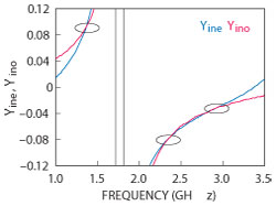
Figure 3 Even- and odd-mode admittances.
The filter’s S-parameters can be derived by (11) and (12).8,9
The condition for stopband transmission zeros is |S21|=0, so the transmission zeros can be found by

Equation 13 can be solved graphically. Figure 3 depicts equation 13 as frequency functions. The filter’s transmission zeros correspond to the intersection points. Because Figure 3 has three intersection points, the filter has three transmission zeros.
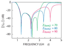
Figure 4 S21 for different values of Z0om2.
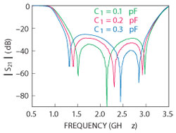
Figure 5 S21 for different values of C1.
Figure 4 illustrates the effect on filter response (S21), including the transmission zero frequencies, due to changes in the intermediate coupling line characteristic impedance (Z0om2). With increasing odd-mode impedance, the first transmission zero remains basically the same, suppression at the second transmission zero decreases slightly, the third transmission zero dramatically shifts higher in frequency, and the bandwidth becomes wider. Suppression at the first zero is unchanged, while suppression at the third zero is reduced. (Z0om2 Z0em2 = 11,200 Ω2, C2 = 4.2 pF, C1 = 0.24 pF, Z0L = Zom1 = ZOU =120Ω, θU = 62°, θL = 11°, θ1 = 11, θ2 = 32°).
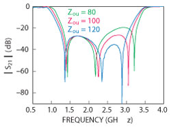
Figure 6 Computed responses of the WBSF with different Z0U.
Figure 5 shows how S21 is influenced by the value of the coupling capacitor C1. When increased, suppression at the first zero decreases, while rejection at the third zero increases. The frequencies of all three transmission zeros shift. Frequencies at the band extremes shift downward, while the frequency of the middle transmission zero increases. The bandwidth remains unchanged. (C2 = 4.2 pF, Z0L = Zom1 = ZOU = 120Ω, Z0om2 = 158Ω, Z0em2 = 71Ω, θU = 62°, θL = 11°, θ1 = 11°, θ2 = 32°).
Figure 6 shows how S21 is influenced by the characteristic impedance of Z0U. With increasing characteristic impedance, suppression at high end of the band increases, leaving suppression at the lower extreme of the band relatively unchanged. The frequency of the second transmission zero increases with increasing Z0U, while the frequency of the third transmission zero decreases. The first transmission zero also decreases, but at a lower rate, therefore, the bandwidth decreases. (Z0L = Zom1 = 120 Ω, Z0om2 = 158 Ω, Z0em2 = 71 Ω, θU = 62°, θL = 11°, θ1 = 11°, θ2 = 32°, C2 = 4.2 pF, C1 = 0.24 pF).
From the above observations, adjusting the value of the coupling capacitor (C1) appears to be the most effective way to control the attenuation poles, because changes to Z0om2 and Z0U have a significant effect on only one transmission zero.
Filter Design And Measurements
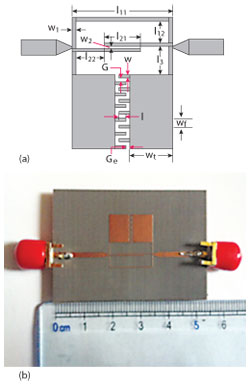
Figure 7 WBSF layout (a); photograph (b).
Based on the analysis, a WBSF having a 20 dB FBW of 89.5 percent at f0 = 2 GHz is designed on a 0.5 mm substrate with a relative dielectric constant of 2.65 and loss tangent 0.002 (see Figure 7). The impedance values of the filter are Z0U = Z0L = Zom1 = 120 Ω, Z0om2 = 158 Ω, Z0em2 = 71 Ω, and corresponding electrical lengths are θU = 62°, θL = 11°, θ1 = 11°, θ2 = 32°. The coupled line’s corresponding width and separation are both approximately 0.2 mm. In addition, two microstrip patches with an interdigital structure are employed to realize the pi network model consisting of three capacitors. C1 and C2 are 0.24 pF and 4.2 pF, respectively. Using Agilent’s ADS, the dimensions of the interdigital structure are determined to be l = 0.6 mm, w = 0.35 mm, wt = 7 mm, wf = 1 mm, G = 0.3 mm and Ge = 0.4 mm. Figure 7(b) is a photograph of the fabricated filter.
The results of simulation (using Ansoft HFSS) and measurement (see Figure 8) show good agreement. The three transmission zeros are located at 1.39 GHz (with a suppression of 46 dB), 2.14 GHz (with a suppression of 55 dB) and 2.89 GHz (with a suppression 53 dB). This provides a wide stopband response with a center frequency of 2 GHz. The lower and upper 3 dB cut-off frequencies are 0.88 and 3.22 GHz, representing a 3 dB FBW of 114.1 percent centered at 2.05 GHz. Rejection is better than 20 dB from 1.20 to 2.99 GHz, corresponding to a 20 dB fractional bandwidth (FBW) of 87.3 percent.
Attenuation rates at the band edges are 67.57 dB/GHz (5 dB at 0.94 and 30 dB GHz at 1.31 GHz) and 78.12 dB/GHz (5 at 3.17 and 30 dB at 2.85 GHz) on the lower and upper side of the stopband, respectively. Furthermore, the filter exhibits good passband performance; the insertion loss is less than 1 dB from DC to 0.76 GHz, and less than 1.1 dB in the upper passband from 3.36 to 3.78 GHz. If the feed lines are not taken in account, the whole filter occupies a compact size of 15.4 × 14.1 mm corresponding to 0.022λg2 (0.155λg × 0.145λg), where λg is the guided wavelength of a 50 Ω transmission line at the center frequency of 2.05 GHz.
Conclusion
A new type of compact bandstop filter using an interdigital capacitor in the parallel-coupled transmission line section achieves deep rejection and a wide bandstop. With the aid of transmission line modeling and simulation, the parameters of the WBSF are derived. By adjusting the value of transmission line characteristic impedances and the value of the coupling capacitor, the bandwidth and rejection level of the stopband can be easily controlled. The filter produces three stopband transmission zeros and, as a result, provides improved rejection in terms of sharpness and attenuation leve.
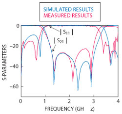
Figure 8 Simulation vs. measurement.
Acknowledgment
The authors wish to acknowledge the support of the National Natural Science Foundation of China under grant (61101052), Zhejiang Provincial Natural Science Foundation under grant (Y1110297) and the Scientific Research Foundation of Zhejiang Sci-Tech University (1004811-Y).
References
- G. Matthaei, L. Young and E.M.T. Jones, Microwave Impedance-Matching Networks and Coupling Structures, Artech House, Norwood, MA, 1980.
- K. Qian, “Compact Wideband Bandstop Filter Using Embedded Capacitor,” Microwave and Optical Technology Letters, Vol. 54, No. 6, June 2012, pp. 1511–1514.
- M.K. Mandal, K. Divyabramham and S. Sanyal, “Compact, Wideband Bandstop Filters With Sharp Rejection Characteristic,” IEEE Microwave and Wireless Components Letters, Vol. 18, No. 10, October 2008, pp. 665-667.
- H. Shaman and J.S. Hong. “Wideband Bandstop Filter with Cross-Coupling,” IEEE Transactions on Microwave Theory and Techniques, Vol. 55, No. 8, August 2007, pp. 1780-1785.
- M.A. Sanchez-Soriano, G. Torregrosa-Penalva and E. Bronchalo, “Compact Wideband Bandstop Filter With Four Transmission Zeros,” IEEE Microwave and Wireless Components Letters, Vol. 20, No. 6, June 2010, pp. 313-315.
- H.K. Chiou and C.F. Tai, “Dual-Band Microstrip Bandstop Filter Using Dual-Mode Loop Resonator,” Electronics Letters, Vol. 45, No. 10, May 2009, pp. 507-509.
- M.K. Mandal and P. Mondal, “Design of Sharp-Rejection, Compact, Wideband Bandstop Filters,” IET Microwaves Antennas & Propagation, Vol. 2, No. 4, January 2008, pp. 389-393.
- D.M. Pozar, Microwave Engineering, 2nd edition, Wiley, New York, 1998.
- J.S. Hong and M.J. Lancaster, Microstrip Filters for RF/Microwave Applications, Wiley,New York, 2001.

Ting Lang is currently working toward the electronic and information engineering bachelor’s degree at the school of Qixin, Zhejiang Sci-Tech University, China. Her research interests include microwave passive circuit design and its applications.

Lin Li received both his bachelor’s and master’s degrees at Zhejiang University and his PhD at Shanghai Jiaotong University. He is currently an associate professor at Zhejiang Sci-Tech University. His research interests include microwave passive circuit design and its applications.

Li-Li Yang is currently working toward the communication engineering bachelor’s degree at the school of Qixin, Zhejiang Sci-Tech University. Her research interests include microwave passive circuit design and its applications.

Zhi-Hao Zhang is currently working toward the communication engineering bachelor’s degree at the school of Qixin, Zhejiang Sci-Tech University. His research interests include microwave passive circuit design and its applications.