
Engineers in the defense community have long sought to replace the bulky and heavy traveling wave tubes (TWT) used in high power systems such as radar, communications satellite and electronic warfare (EW) with compact, lightweight, cheaper and more efficient semiconductor components.1 Semiconductors also enable system level features like phased array radars. More than any other semiconductor material, GaN exhibits intrinsic properties that make it as promising as a TWT replacement;2 its wide band gap enables high voltage operation and high power added efficiencies (PAE). However, thermal limitations have so far impeded the industry’s progress toward GaN’s optimal performance as GaN’s RF power is increased.3
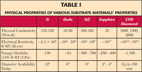
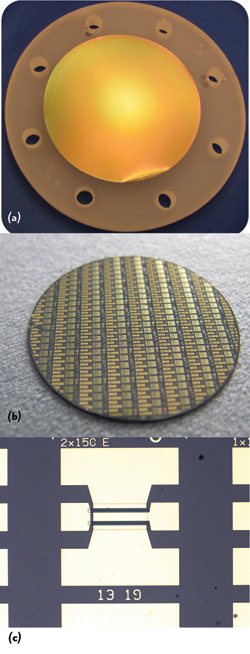
Figure 1 Photo of an unprocessed 4-inch GaN-on-diamond wafer (a), a photo of 1-inch GaN-on-Diamond wafer processed into HEMTs by AFRL4 (b), and a photo of a 2-finger GaN-on-diamond HEMT4 (c).
It has been shown via modeling and preliminary device demonstrations that replacing GaN’s host substrate (typically SiC) with directly deposited CVD diamond would boost RF area power density three-fold compared to GaN-on-SiC.4-6 Heat is extracted via bottom thermal conduction. The three-fold boost to power density derives from the 40 percent reduction in the transistor’s channel temperature rise compared to GaN-on-SiC; at a reduced channel temperature rise, the GaN’s transistor gate fingers may be brought three times closer together without fear of thermal cross-talk. Table 1 compares the electrical and thermal properties of diamond with other substrates typically used to host GaN.5 Note that diamond’s thermal conductivity is about five times greater than that of SiC. Diamond is also an excellent electrical insulator – a property needed for high frequency power amplifiers. Additionally, the spatially shrunken GaN-on-diamond devices can operate amidst a much higher ambient temperature compared to GaN-on-SiC. This is due to the reduced thermal impedance stack between the GaN channel and the substrate/package. Key to the success of GaN-on-diamond is that the diamond can be grown to within tens of nanometers of the GaN epitaxy maximizing its heat spreading function.
GaN-on-diamond PAs also hold promise for use in cellular base stations where operating energy costs in cooling the PAs can be significant for service providers. GaN-on-diamond’s ability to operate in a much higher ambient temperature and at a higher PAE than any other semiconductor material translates into direct costs savings from reduced physical space, smaller power supplies and less energy use.
Making GaN-on-Diamond Epitaxial Wafers
GaN-on-diamond wafers are shown in Figure 1. The AlGaN/GaN HEMT layer structure was grown by metal-organic chemical vapor deposition (MOCVD) on a high resistivity Si (111) substrate. Starting from the Si substrate, epitaxial layers included a 1.1 µm thick proprietary transition buffer, an 800 nm thick undoped GaN buffer layer, a 17 nm thick Al0.26Ga0.74N Schottky barrier, and a 2 nm GaN cap layer. A 100 µm thick CVD diamond layer was grown on a dielectric-coated GaN epitaxial substrate (GaN buffer, AlGaN barrier and GaN cap). The process for diamond growth is as follows: the host Si (111) and transition layers beneath the AlGaN/GaN epitaxy are removed, a 50 nm thick proprietary dielectric is deposited onto the exposed AlGaN/GaN and finally a 100 µm thick CVD diamond substrate is grown onto the dielectric adhering to the epitaxial AlGaN/GaN films.
In understanding whether the GaN-on-diamond wafer formation process used here negatively affected the GaN epitaxy, numerous tests were conducted on the GaN epitaxy including high-resolution X-ray, CV, Lehighton, Low-Temp PL, Hall and TEM. Those test results were reviewed before and after the diamond deposition on the GaN epitaxy.7 None of the tests could detect any changes to the GaN epitaxy. Table 2 shows the result of high-resolution X-ray tests on GaN-on-diamond wafers; no changes to the lattice constant (d0002) of the GaN epitaxy were resolvable and the aluminum compositions (XAl) were nearly identical (to within 1 percent).
Measured GaN-on-Diamond DC and RF Results
TriQuint Semiconductor fabricated the GaN-on-diamond RF HEMT devices discussed in this article, the details of which have been already published.5,8 Then the company characterized the DC electrical performance of the fabricated devices, measuring an electron mobility of 1400 cm2/V-s, a sheet charge density of 9.6×1012 cm-2, and a sheet resistance of about 440 Ω/sq on the GaN-on-diamond wafers. The 50 µm gate-width HEMT drain-current measurements show excellent pinch-off characteristics and a maximum current density of about 1100 mA/mm. Figure 2 depicts the DC transfer characteristics of the same device at a drain voltage of 10 V; measurements of peak transconductance gave 300 mS/mm and a threshold voltage of –3.4 V. Measurements of the gate-drain breakdown voltage across 10 sample devices, at a gate-drain current of 1 mA/mm, varied between 25 and 52 V. It is suspected that the wafer surface preparation process, still under development, at the time, may have caused this breakdown voltage variation; isolation currents measured between two mesa patterns with ohmic contacts and a spacing of 5 µm indicated very low buffer leakage current with < 10 µA/mm at a maximum applied voltage of 80 V.
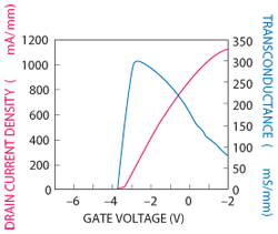
Figure 2 Transfer characteristics of a 50 µm GaN-on-diamond HEMT at a drain voltage of 10 V.
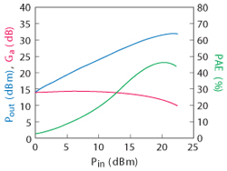
Figure 3 10 GHz CW load-pull results of a 2 × 100 µm GaN-on-diamond HEMT.
To characterize RF performance, continuous wave (CW) load pull tests of 2×100 µm gate width HEMTs at 10 GHz were conducted using a Focus Microwave test setup. Devices biased at a quiescent drain voltage of 40 V and a drain current of 100 mA/mm were tuned for peak PAE. Figure 3 shows the measured input-output power response with a peak PAE of 46.7 percent at 20 dBm of input power (Pin). The device was tuned for PAE at a drain voltage of 40 V and a quiescent drain current density of 100 mA/mm. At the PAE peak, the output power (Pout) is 31.7 dBm (7.4 W/mm) and associated gain is 11.7 dB. At 28 V drain voltage, an output power of over 5 W/mm along with a PAE of about 55 percent was achieved. To the authors’ best knowledge, these results demonstrate the highest RF power for GaN-on-diamond HEMTs at 10 GHz and are equivalent to the maximum power ever extracted from the same epitaxy and device structure.9 The high leakage current that caused the variation in breakdown voltage mentioned earlier also makes the PAE in these devices lower than expected; the authors believe that reducing the leakage will significantly increase the PAE. Adding a source connected field plate in the channel is also expected to improve the high voltage performance of these devices. This improvement work is in progress, and a comprehensive report, including thermal performance, will be published in the future.
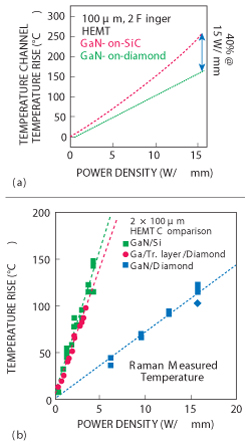
Figure 4 Peak channel temperature derived from micro-Raman measurements on GaN-on-diamond and GaN-on-SiC HEMTs (a) and peak channel temperatures of GaN-on-diamond HEMTs compared to GaN-on-Si, and GaN-on-diamond where the transition layers have not been removed (b).
Thermal Measurements of GaN-on-Diamond HEMTs
Peak temperatures shown here have been calculated using measured micro-Raman temperatures. Thermal performance evaluation of GaN-on-diamond devices was done using micro-Raman spectroscopy. Details of the micro-Raman technique are presented by Pomeroy et al.10 The spot size measured with the micro-Raman technique is about 1 µm3 from the surface of the GaN adjacent to the gate between the drain and the gate. Test HEMTs with gate width of 2×100 µm and TLM structures with 100 µm width and 20 µm spacing were used to measure the channel temperature rise at different DC power dissipation conditions. For comparison, TriQuint’s standard 100 µm thick 2×100 µm GaN-on-SiC HEMTs were also tested using the micro-Raman technique. According to the measurements (see Figure 4), GaN-on-diamond HEMTs exhibited an approximately 40 percent lower thermal resistance or ~160°C per W/mm compared to GaN-on-SiC. Figure 4 also shows that the thermal resistance of GaN-on-diamond HEMTs as nominally made with no transition layers between GaN and diamond is lower by over four times than GaN-on-Silicon or GaN-on-diamond with the transition layers still included between GaN and diamond (trends lines are included for illustrative purposes).
The reduction in the GaN thermal resistance shown is attributed to a) the high thermal conductivity diamond situated in close proximity (~1 µm) of the hot GaN HEMT junction, and b) the removal of defective transition layers of GaN-on-Si beneath the AlGaN/GaN films. Simulations show that a 40 percent reduction in thermal resistance could enable 2.5 to 3× increases in the density of gates (or output power) in a power amplifier, as well as significant reductions in the cost of cooling – since the transistor may be allowed to operate at a higher ambient temperature. Note that in this work, the GaN’s gate fingers were not brought closely together compared to GaN-on-SiC – a key feature that is now possible by the reduced channel temperature rise.
Reliability Measurements
With GaN resting on a new foreign substrate – and one whose thermal expansion coefficient, crystal structure, surface properties, and internal stress are very different from that of GaN – device reliability becomes a concern for engineers using GaN-on-diamond. In an effort to assess the reliability question seven GaN-on-Si and 12 GaN-on-diamond HEMT, devices were subjected to channel temperatures of up to 350°C with a constant source-drain voltage of up to 24 V.11 The source-drain current and the gate leakage current were monitored during the endurance tests. After 3000 hrs at a 350°C channel temperature, 9000 hrs at 290°C, and 17000 hrs at 215°C, the authors were unable to quench the GaN-on-diamond HEMTs; in contrast, all the control GaN-on-Si devices, sharing the same GaN epitaxy and device structure as the GaN-on-diamond devices, catastrophically failed.11
Figure 5 shows the endurance results measured from GaN-on-Si and GaN-on-diamond HEMT devices. In the tests, all the GaN-on-Si and GaN-on-diamond devices were subjected to a 24 V DC bias (source-drain) for 5000 hrs at a 215°C channel temperature. During this 5000 hr period, the drain currents of both GaN-on-Si and GaN-on-diamond devices declined slowly (not shown here); detailed analysis of this behavior has been published.11 The channel temperatures of all the aforementioned devices were then increased to 350°C; almost immediately, the GaN-on-Si drain-source current began a precipitous drop. The GaN-on-diamond device currents remained relatively flat in the same period that GaN-on-Si dropped.

Figure 5 Source-drain current measured from GaN-on-Si HEMTs (a) and GaN-on-diamond HEMTs (b) while all the devices' channel temperatures were maintained at 350°C (source-drain voltages were 24 V).
The graphs shown in Figure 5 began after the initial 5000 hrs soak at 215°C. After 100 hrs at 350°C, all the GaN-on-Si devices dropped 20 percent or more from their starting point. The GaN-on-diamond devices remained generally flat at 1000 hours when all the tests were terminated for logistics reasons. The results are virtually identical for devices biased at channel temperatures of 290°C as published in the literature.11 Unable to completely terminate any of the GaN-on-diamond devices during the tests – due to their robustness, the GaN-on-diamond’s activation energy could not be calculated. The authors point out that the starting currents of the GaN-on-diamond devices shown in Figure 5 are generally lower than the GaN-on-Si devices; this is due to variations in wafer processing of the wafers. The authors believe that the relatively low level of the current densities in the device will have little affect on the outcome of the tests.
Impact on Systems
In the design of radar, EW, radio jammer, satellite communications, naval and avionics systems, two critical GaN-on-diamond features distinguish the material from other semiconductors. First, GaN-on-diamond devices exhibit a total thermal resistance (traversing the HEMT’s gate down to the substrate) that is 40 percent less than the industry benchmark GaN-on-SiC HEMTs;12-16 there are variations in the numbers due to use of different measurement techniques, which will be better understood in the months ahead. Secondly, GaN-on-diamond devices also exhibit a reduced lateral thermal profile and cross talk; this latter parameter is due to the effective heat spreading of diamond.
Impact on Cooling Costs – A semiconductor’s thermal resistance is an important parameter in the design of a microelectronic system because it determines the resilience of the system to high ambient temperatures. For instance, consider two devices that exhibit the same channel temperature of 200°C: device A (GaN-on-diamond) harbors a thermal resistance of 10°C/W, and device B (GaN-on-SiC) harbors 20°C/W. Assuming a 5 W power dissipation along the GaN-on-substrate stack, device A will exhibit a 50°C temperature drop between the gate and the substrate (leaving the substrate at 150°C), whereas device B will exhibit 100°C between the same points (leaving the substrate at 100°C). In other words, whereas both devices are firing at the same channel temperature producing the same RF power, the GaN-on-diamond substrates, packages, and ambient temperatures can be allowed to operate 50°C hotter simply because its thermal resistance is lower by 50 percent. In practice, the costs of maintaining a complex electronics system’s ambient temperature at 100°C (device B) as opposed to allowing it to operate hotter at 150° or 166°C (device A) can be prohibitive. For numerous applications, this feature can be enabling and strategic.
Impact without Cooling – If devices A (GaN-on-diamond) and B (GaN-on-SiC) described previously are allowed to float at the same ambient temperature without active cooling, then compared to device B, the lower thermal resistance of device A would equate to a much lower channel temperature while the device A is firing. In the scenario described above, device A would for instance operate at 133° to 150°C whereas device B would operate at 200°C – while producing the same RF power. The impact of this reduced operating temperature is quite profound for the system since RF power amplifiers lay at the core of many of RF electronic systems including radar, EW, avionics, jammers, etc. Reliability-related parameters of activation energy, mean-time-to-failure, and lifetime all derive directly and exponentially from operating temperature.17 Substantial energy savings for the system operator can be had over a 20 to 30 year system lifetime of operating costs that requires less use of energy.
Impact on Power Amplifier, Power Density and Costs – The reduced lateral thermal crosstalk of GaN-on-diamond devices enables higher power densities. Various groups have recently shown that the GaN HEMT gate fingers on diamond can be brought nearly threefold closer together on diamond than on SiC.8,15 This 3× tighter gate finger separation equates to a 3× greater RF power density from the packaged device, enabling the cost per watt for GaN-on-diamond to be close to 3× lower than GaN-on-SiC; a wafer customer need only process one GaN-on-diamond wafer rather than three GaN-on-SiC wafers to achieve the same RF output power. Fab process costs would be saved from the fewer runs.
Impact on Low Power Devices – In the case of smaller electronics systems or low power electronics (under 50 W), power densities can still soar (~kW/mm2) since gate feature sizes are small (~ microns) – begging the need for effective materials-level thermal management.
Conclusion
High-quality GaN-on-diamond wafers have demonstrated whereby the crystal quality of the GaN epitaxy is virtually identical to the original layers as grown on SiC substrates. State-of-the-art HEMTs made on GaN-on-diamond wafers show excellent electrical DC and RF properties, along with a clear thermal improvement over current GaN-on-SiC HEMTs. Preliminary high-temperature operating life test data collected by the authors over a 7 to 24 month period show a clear reliability improvement in GaN-on-diamond devices compared to the control GaN-on-Si devices which produced the original GaN epitaxy. The GaN-on-diamond HEMTs at 290° and 350°C channel temperatures never failed while all of the control GaN-on-SiC devices failed at the same temperatures within dozens of hours.
Various parties have also begun to quantify the extent of GaN-on-diamond’s thermal benefits. GaN-on-diamond’s lower channel temperature and its lower thermal impedance (40 percent lower than GaN-on-SiC) will lead to a) reduced $ per watt components due to more devices per wafer, b) reduced system cooling costs – both fixed costs, and operating expenses – due to a higher allowable ambient temperature, c) reduced size of the power amplifier and its related parts; this is noteworthy for low power devices (< 10 W) and applications where space is a premium, and d) reduced size and weight at the system level where cooling apparatus are typically bulky and heavy.
Acknowledgment
This work was sponsored by DARPA’s Near Junction Thermal Transport (NJTT) effort, which is managed by Dr. A. Bar-Cohen, and supported by Dr. J. Felbinger, Dr. J. Maurer and Dr. A. Kane. This work was also sponsored by the Navy SBIR Phase-II Topic # N08-170 program managed by
C. Pagel. The authors also acknowledge M. Kubal of Bristol University for the Micro Raman thermal measurements shown here. Distribution Statement A (Approved for Public Release, Distribution Unlimited).
References
- “Electronic Warfare and Radar Systems Engineering Handbook,” by NAVAIR Electronics Warfare/Combat Systems, Rev 4 of June 1, 2012. (Unclassified, Approved for public release).
- O. Madelung, Semiconductors – Basic Data, Ed., Springer, 2nd revised Edition, 1996.
- G.J. Riedel, J.W. Pomeroy, K.P. Hilton, J.O. Maclean, D.J. Wallis, M.J. Uren, T. Martin, U. Forsberg, A. Lundskog, A. Kakanakova-Georgieva, G. Pozina, E. Janzen, R. Lossy, R. Pazirandeh, F. Brunner, J. Wurfl and M. Kuball, “Reducing Thermal Resistance of AlGaN/GaN Electronic Devices Using Novel Nucleation Layers,” IEEE Electron Device Letters, Vol. 30, No. 2, February 2009, pp. 103-106.
- G.D. Via, J.G. Felbinger, J. Blevins, K. Chabak, G. Jessen, J. Gillespie, R. Fitch, A. Crespo, K. Sutherlin, B. Poling, S. Tetlak, R. Gilbert, T. Cooper, R. Baranyai, J.W. Pomeroy, M. Kuball, J.J. Maurer and A. Bar-Cohen, “Wafer-Scale GaN HEMT Performance Enhancement by Diamond Substrate Integration,” 10th International Conference on Nitride Semiconductors, ICNS-10, August 25-30, 2013, Washington DC, USA.
- D.C. Dumka, T.M. Chou, F. Faili, D. Francis and F. Ejeckam, “AlGaN/GaN HEMTs on Diamond Substrate with Over 7 W/mm Output Power Density at 10 GHz,” Electronics Letters, Vol. 49, No. 20, September 26, 2013, pp. 1298-1299.
- H.C. Nochetto, N.R. Jankowski and A. Bar-Cohen, “GaN HEMT Junction Temperature Dependence on Diamond Substrate Anisotropy and Thermal Boundary Resistance,” 34th IEEE Compound Semiconductor IC Symposium (CSIC)October 14-17, 2012, La Jolla, CA, ISSN: 1550-8781, pp. 1-4.
- F. Ejeckam, D. Francis, F. Faili and D. Babic, “GaN-on-Diamond Semiconductors,” in a final project AFRL report for Contract # FA8650-09-C-5404, March 2012.
- D.C. Dumka, T.M. Chou, J.L. Jimenez, D.M. Fanning, D. Francis, F. Faili, F. Ejeckam, M. Bernardoni, J.W. Pomeroy and M. Kuball, “Electrical and Thermal Performance of AlGaN/GaN HEMTs on Diamond Substrate for RF Applications,” 35th IEEE Compound Semiconductor IC Symposium (CSIC), October 13-16, 2013, Monterey, CA, Section F.4.
- D.C. Dumka and P. Saunier, “GaN on Si HEMT with 65% Power Added Efficiency at 10 GHz,” IEEE Electronics Letters, 2010, Vol. 46, No. 13, pp. 946-947.
- J. Pomeroy, M. Bernardoni, A. Sarua, A. Manoi, D.C. Dumka, D.M. Fanning and M. Kuball, “Achieving the Best Thermal Performance for GaN-on-Diamond,” 35th IEEE Compound Semiconductor IC Symposium (CSICS)October 13-16 2013, Monterey, CA, Section H.4.
- F. Ejeckam, D. Babic, F. Faili, D. Francis, F. Lowe, Q. Diduck, C. Khandavalli, D. Twitchen and B. Bolliger, “3,000+ Hours Continuous Operation of GaN-on-Diamond HEMTs at 350°C Channel Temperature,” Accepted for publication to Semi Therm Conference,March 9-13, 2014, San Jose, CA.
- J. Felbinger, M.V.S. Chandra, Y. Sun, L.F. Eastman, J. Wasserbauer, F. Faili, D. Babic, D. Francis and F. Ejeckam, “Comparison of GaN HEMTs on Diamond and SiC Substrates,” IEEE Electron Device Letters, Vol. 28, No. 11, November 2007, pp. 948.
- Y. Won, J. Cho, D. Agonafer, M. Asheghi and K.E. Goodson, “Cooling Limits for GaN HEMT Technology (Invited),” 35th IEEE Compound Semiconductor IC Symposium (CSIC)October 13-16, 2013, Monterey, CA, Section F.1.
- J. Pomeroy, M. Bernardoni, A. Sarua, A. Manoi, D.C. Dumka, D.M. Fanning and M. Kuball, “Achieving the Best Thermal Performance for GaN-on-Diamond,” 35th IEEE Compound Semiconductor IC Symposium (CSIC),October 13-16 2013, Monterey, CA, Section H.4.
- M. Tyhach, D. Altman and S. Bernstein, “Analysis and Characterization of Thermal Transport in GaN HEMTs on SiC and Diamond Substrates,” submitted to GOMACT 2014.
- D.C. Dumka, T.M. Chou, J.L. Jimenez, D.M. Fanning, D. Francis, F. Faili, F. Ejeckam, M. Bernardoni, J.W. Pomeroy and M. Kuball, “Electrical and Thermal Performance of AlGaN/GaN HEMTs on Diamond Substrate for RF Applications,” 35th IEEE Compound Semiconductor IC Symposium (CSIC),October 13-16 2013, Monterey, CA, Section F.4.
- J.A. del Alamo and J. Joh, “GaN HEMT Reliability,” 20th European Symposium on the Reliability of Electron Devices, Failure Physics and Analysis, Vol. 49, Issue 9-11, September-November 2009, pp. 1200-1206.