
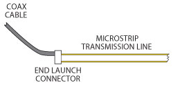
Figure 1 Signal launch from a coaxial cable and connector to a microstrip.
Transferring high frequency energy from a coaxial connector to a printed circuit board (PCB) is often referred to as a signal launch and it can be difficult to characterize. How efficiently energy is transferred can vary a great deal from one circuit structure to another. Factors such as the PCB material, its thickness and the operating frequency range affect performance, as well as the connector design and its interaction with the circuit material. With an understanding of the issues, including the differences in signal-launch configurations, and by reviewing some examples of ways to optimize RF/microwave signal launches, performance can be improved.
Achieving an effective signal launch is design dependent, with broadband optimization typically more challenging than narrowband. Design of a high frequency launch usually grows in difficulty with increasing frequency, and can be more problematic with thicker circuit materials and more complicated circuit constructions.
Signal Launch Design and Optimization
A signal launch from a coaxial cable and connector to a microstrip PCB is illustrated in Figure 1. The electromagnetic (EM) fields traveling through the coaxial cable and connector have a cylindrical orientation while the EM fields in the PCB have a planar or rectangular orientation. When the fields transition from one propagating medium to another, they change orientation to accommodate the new environment, causing anomalies. The transition depends upon the type of medium; whether a signal launch is being made, for example, from a coaxial cable and connector to microstrip, grounded coplanar waveguide (GCPW), or stripline. The type of coaxial connector also plays an important role.
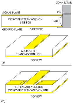
Figure 2 Representation of a thick microstrip transmission line circuit and the lengthened ground return path back to the connector (a), a grounded coplanar launched microstrip circuit (b).
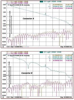
Figure 3 Coplanar launch microstrip circuit tested with similar end launch coaxial connectors having different ground separations.
Optimization may involve several variables. Understanding the EM field orientation within a coaxial cable/connector can be useful, but the ground return path must also be considered as part of the propagating medium. It is often beneficial to achieve smooth impedance transitions from one propagating medium to another. Knowing the capacitive and inductive reactances at impedance junctions can provide insights into the expected behavior. When three-dimensional (3D) EM simulation is available, current-density mapping can be used. In addition, best practices associated with radiation loss can serve as guidelines.
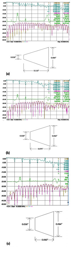
Figure 4 Performance of three microstrip circuits with different tapers; the original design having a long narrow taper (a), the taper length reduced (b), and the taper length reduced still further (c).
Although the ground return path between a signal launch connector and a PCB may not appear to be an issue, the ground return path from the connector to the PCB are ideally continuous and uninterrupted; this may not always be the case. There is typically some small surface resistance between the metal of the connector and the PCB. There may also be small conductivity differences between the solder that joins the different parts and the metal of those parts. These small differences usually have minor effects at lower RF and microwave frequencies, but they can significantly affect performance at higher frequencies. The actual length of the ground return path can play a role in the quality of launch that is achieved with a given connector and PCB combination.
As Figure 2a illustrates, when EM energy transitions from a connector pin to the signal conductor of a microstrip PCB, the ground return path back to the connector housing can be lengthy for a thick microstrip transmission line. Using a PCB material with a relatively high dielectric constant can exaggerate the problem by leading to a longer electrical length in the ground return path. Any lengthening of this path can result in frequency-dependent issues typically linked to a localized difference in phase velocity and capacitance. Both are related and affect the impedance in the transition area and cause differences in return loss. Ideally, the length of a ground return path should be minimized, with no impedance anomalies in the signal launch area. Note that the grounding point of the connector in Figure 2a is shown only on the bottom of the circuit. This is a worst-case scenario. Many RF connectors have grounding pins on the same layer as the signal. In that case, the PCB will have ground pads there, as well.
Figure 2b represents a coplanar launched microstrip circuit, where the body of the circuit is microstrip but the signal launch area is a grounded coplanar-waveguide (GCPW). Coplanar launched microstrip is advantageous because it minimizes the ground return path and has other beneficial properties. When using a connector with ground pins on both sides of the signal conductor, the ground pin separation distance can have a significant impact on performance. It has been demonstrated that this distance impacts the frequency response.1
In an experiment with a coplanar launched microstrip on 10-mil-thick RO4350B™ laminate from Rogers Corp., similar connectors are used, but with different ground spacings at their coplanar launch interfaces (see Figure 3). Connector A has a ground separation of approximately 0.030", while Connector B has a ground separation of 0.064". The connectors launch onto the circuit the same in both cases.
The x-axis shows frequency, with each division representing 5 GHz. Performance is comparable at lower microwave frequencies (< 5 GHz), but above 15 GHz, performance of the circuit with wider ground separation degrades. The connectors are similar, although there is a slight difference in pin diameters between the two models, Connector B has a larger pin diameter and is designed for use with a thicker PCB material. This may also have contributed to the performance differences.
A simple and effective method for optimizing signal launch is to minimize impedance mismatches in the signal launch area. A rise in the impedance curve is basically due to an increase in inductance while a dip in the impedance curve is due to an increase in capacitance. For the thick microstrip transmission line shown in Figure 2a (assuming a PCB material with a relatively low dielectric constant of about 3.6), the conductor is relatively wide – much wider than the connector’s center conductor. With a large dimensional difference between the circuit’s conductor and the connector’s conductor, there is a strong capacitive spike at the transition. This can often be reduced by tapering the circuit’s conductor to form a more narrow transition where it joins with the coaxial connector pin. Narrowing the PCB conductor makes it more inductive (or less capacitive), offsetting the capacitive spike in the impedance curve.
Frequency-dependent effects must be considered. A taper occurring over a long distance provides a greater inductive effect at lower frequencies than a shorter taper. For example, in the case of a signal launch with poor return loss at lower frequencies and having a capacitive impedance spike, a longer taper may be suitable. Conversely, a short taper has a greater effect on higher frequencies.
For a coplanar-launched geometry, the adjacent ground planes can increase the capacitance when they are close to the signal conductor. Frequency-dependent adjustments are often made through the combinations of signal taper and ground plane spacing to modify the inductance and capacitance of the signal launch as required. In some cases, the coplanar spacing is wide over a certain distance of the taper, correlating to some band of lower frequencies. The spacing then narrows at a wider portion of the taper and over a short distance to affect higher frequencies. In general, narrowing the conductor taper adds inductance. The length of the taper affects the frequency response. Altering the adjacent coplanar ground spacing changes the capacitance and the distance of the adjacent spacing influences the frequency band over which the change in capacitance is most effective.
Examples
Figure 4 provides a simple example. Figure 4a is a thick microstrip transmission line with a long and narrow taper. The taper is 0.018" (0.46 mm) wide starting at the edge of the circuit and over a length of 0.110" (2.794 mm), it transitions to the width of a 50 Ω conductor, 0.064" (1.626 mm). The taper is reduced to shorter lengths in Figures 4b and c. Field-serviceable, pressure-contact, end-launch connectors are used and not soldered, so the same connector is used in each case. The microstrip transmission line is 2" (50.8 mm) in length and fabricated on a 30 mil (0.76 mm) thick RO4350B™ microwave circuit laminate, with a dielectric constant of 3.66. In Figure 4a, the blue curve represents insertion loss (S21), with many ripples in the response. In contrast, S21 in Figure 4c has the least number of ripples. As these curves reveal, the trend is for improved performance with shorter taper.
Perhaps the most telling curves in Figure 4 show the impedance of the cables, connectors and circuit (the green curves). The large positive peak in Figure 4a represents the connector on the circuit attached to a cable at port 1. The peak on that same curve to the right is the connector at the other end of the circuit. The large impedance peak is reduced with a reduction in taper length. The improvement of the impedance match in the signal launch areas is due to the taper becoming wider as it is shortened, the increase in taper width correlating with a reduced inductance.
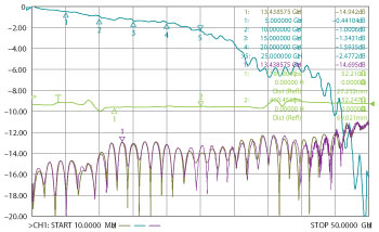
Figure 5 Performance that is further optimized.
An excellent reference on signal launch,2 which uses this same material and material thickness in its examples, offers some further insight into circuit dimensions in the signal launch area. A coplanar launched microstrip built with its recommendations (see Figure 5) yields performance superior to that of Figure 4. The most obvious improvement is elimination of the inductive spike in the impedance curve, which is actually a mix of a slight inductive spike and a slight capacitive dip. Having the correct taper minimizes the inductive spike, while additional capacitance is provided by the coupling of the coplanar line adjacent grounds in the launch area. The insertion loss curve for Figure 5 is smoother than shown in Figure 4c and the return loss curve is also improved. The example in Figure 4 will have a different outcome for a microstrip circuit on a PCB material with higher dielectric constant, or different thickness, or using a different connector style.
Signal launch is a complex issue and can be influenced by many different factors. This example and these guidelines are intended to assist designers in understanding some of the basic principles.
References
- Eric Holzman, Essentials of RF and Microwave Grounding, Artech House, Norwood, MA, 2006.
- Bill Rosas, “The Design and Test of Broadband Launches up to 50 GHz on Thin and Thick Substrates,” Southwest Microwave Inc., Tempe, AZ, 2011, www.southwestmicrowave.com