
To cope with an increasing number of frequency bands and advanced mobile phone standards supporting high data rates, current and future wireless communication systems must satisfy stringent performance expectations while simultaneously being more energy-efficient and having lower operating costs. One major limitation of today’s mobile phones is poor impedance matching of the antenna to the RF front end section resulting in poor antenna efficiency. This is exacerbated by current trends toward higher miniaturization and integration, presenting ever increasing challenges in the design of complex RF systems and the management of RF interaction on signal lines. By introducing tunable RF elements, the overall system architecture can be simplified, leading to significant cost reductions and performance optimization.
This article introduces recent advances in RF MEMS vias that allow 3D signal routing using silicon interposers and make compact, high performance inductors commercially available using a combination of innovative MEMS techniques. This article also discusses why full wafer thickness processing makes the RF performance achievable and introduces advanced research in ferromagnetics, which can boost performance of the inductor component even further.
Performance Requirements for Practical RF IPDs
Current mobile phone designs still rely on discrete surface-mounted passive devices to provide RF signal conditioning throughout the handset. A typical mobile phone can have hundreds of surface-mounted passives yet only 20 to 40 ICs. In a typical mobile phone, the discrete passive components account for 90 percent of the component count, 80 percent of the size and 70 percent of the handset cost.1
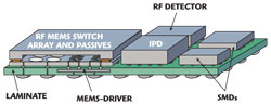
Figure 1 Schematic of front end antenna module.
To date, the industry has responded by reducing the size of the passive components down to a 0402 SMD package size, such as those recently launched by Murata Corp. in Japan.2 The cost of mounting these ultra-miniature SMD devices, however, often negates the component cost savings. Further reductions in size and cost can only come from integrated passive devices (IPD) which can still deliver the performance required by the handset.
Focusing specifically on inductor components, high-Q inductors in the 1 to15 nH range with minimal footprints are needed to build matching networks that can both correct the real as well as the imaginary parts of RF signals present in mobile communications systems. By using a novel 3D through-silicon via (TSV)-based approach, we have shown that both one- and two-port inductors with Q-factors above 30 for the 0.5 to 4 GHz frequency range, while covering an area of about 1 mm2 for inductances of a few nH, are not only achievable, but are practical as the basis for a new class of IPDs. With next generation TSVs currently in development, even further die size reduction to much less than 1 mm2 is possible for the same inductor values.
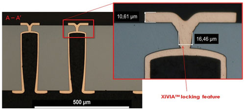
Figure 2 Cross section of Met-Via TSV.
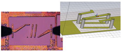
Figure 3 Microphotograph of three-turn 3D inductor being probed, with CAD explosion.
Background
Development of this new type of 3D inductor is pursued under the European Union ENIAC Joint Undertaking EPAMO project, a 15-member consortium to explore and implement a number of innovative process and testing technologies to realize an adaptive 4G radio front end system for mobile phones.3 One of the main building blocks of the front end is the integrated adaptive antenna tuner, consisting of MEMS switches and passive RF 3D-IPDs with TSVs and 3D inductors on thin laminate substrates (schematically shown in Figure 1). The complete module will finally be overmolded. With the availability of adaptive RF tuning in mobile handsets, mobile phone power levels can be reduced by up to 50 percent with no loss in signal strength or integrity. Base station power can also be conserved, with at least 10 percent power savings achievable.
High-Q inductors are needed to build the IPD matching networks. Miniaturized on-chip inductors, therefore, represent critical elements in the overall system. Due to the relatively low Q-factor values currently reported for on-chip semiconductor thin film components (typically in the range of 10 to 20 or lower), the need for new innovative solutions still exists. Addressing this need is one of the major goals of the EPAMO project.
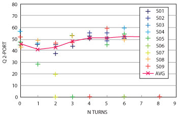
Figure 4 Q-factors at 1 GHz vs. number of turns in the 3D inductor at nine different wafer positions (S01-S09) equally distributed over each tested 8" wafer.
Met-Via®TSV Process
Despite much industry work on thin wafer TSV technologies utilizing wafers as thin as 20 µm (being driven by interposers for 3D IC packaging, among other trends), a high performance 3D RF inductor requires thicker substrates to maximize inductor length, without increasing its IPD footprint. Separating the inductor windings with a thick substrate reduces the capacitive as well as mutual inductance coupling. This allows the fabrication of compact IPD inductors without compromising inductor values or Q factors due to parasitic effects (such as is seen on 2D single-sided or CMOS 2-layer fabricated inductors). This approach is made possible by copper thru-wafer vias in 300 µm thick substrates that meet performance and reliability requirements for high volume commercial use.
The basis for this TSV is the Met-Via process developed at Silex Microsystems.4 This process utilizes XiVia™ Technology from ÅAC Microtec which results in a highly reliable and ruggedized TSV capable of handling demanding temp cycling and operating life requirements. CTE mismatch between the copper and surrounding silicon is large enough that, with repeated temp cycling, a copper TSV can cause de-lamination or cracks in the silicon substrate leading to electrical opens, or breaks, and long term reliability concerns. Met-Via TSVs are all-copper electroplated TSVs with a unique locking structure for TSV reliability (the XiVia structure) as well as a copper-lined TSV topology (as opposed to completely filled TSV). This provides CTE mismatch relief during temperature cycling. The TSV is plated (front and back side) in one plating operation, which is a much more cost effective approach to TSV formation than typical blind via approaches, which require two separate plating operations. The one-step electroplating is what also enables the formation of the new 3D inductor. Figure 2 shows the XiVia structure (the marrying of the small bore from the top with the large bore from below, to create a locking structure for the TSV in silicon).
3D Inductors in Silicon and RF Performance
Inductors using from 1 to 8 turns were fabricated for characterization. Figure 3 is a top-side photomicrograph of a three-turn 3D inductor, with a CAD image of the inductor design (silicon removed for illustration). The 8" wafers with inductors on board were temporarily bonded to a glass substrate to isolate the readings from the effects of the underlying chuck. One- and two-port S-parameters are shown in Figures 4 and 5. Q values, derived from measured Y-parameters, of over 30 at 1 GHz are achieved for all inductor designs. In Figure 5, the inductance value for each inductor design was determined from a fit of a parallel L-C model, with resistive loss in the L section, to the series branch of a pi-model of the measurement data. The series and two parallel branches were determined, by direct calculation, from the Y-parameters. The inductors were characterized out to 10 GHz and practical RF inductors for frequencies up to 3.6 GHz were successfully demonstrated as well. Stable inductor performance was demonstrated up to 100°C. The self-resonance frequency (SRF) depends on the number of turns. For 1 to 6 nH inductors, an SRF of above 10 GHz is achieved. The authors are working on further improving this performance by integrating magnetic core material.
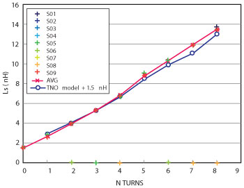
Figure 5 Inductance values at 1 GHz vs. number of turns in the 3D inductor structure at nine different wafer positions (S01-S09) distributed over each tested 8" wafer compared with theoretical modeling.
IPD vs SMD Inductors
To benchmark the 3D-IPD inductors vs. commercially available SMD inductors for RF front end applications, the RF MEMS group at KTH has done modeling and designs of various 3D-IPD inductors using the Silex Met-Via RF 3D-IPD process and compared these designs to existing device models.5 Figure 6 illustrates three different TSV inductors designed to match a 2.7 nH inductor from Murata (LQW15AN2N7C00). Electromagnetic simulations of the inductors were performed using CST Microwave Studio and the frequency response of the Murata reference inductors was modeled in Agilent ADS. Very good inductance matching in the 0.4 to 2 GHz frequency regime is obtained with Silex 3D inductors having an SRF in the 9 GHz range and, depending on inductor design, Q-values in the 60 to 120 range are achieved over the frequency regime of interest.
Ferromagnetics: Pushing the Performance Boundary
With process support from Oerlikon Systems in Lichtenstein and Veeco Instruments in the U.S., the authors have developed a material platform for utilizing nickel-iron (NiFe) magnetic films for the first time at GHz frequencies.
On-chip integrated inductors, currently with a maximum inductance density of some few tens of nH/mm2, would benefit from magnetic materials that significantly reduce the required area. At DC to approximately 10 MHz, the relative permeability of NiFe layers is reported to be as high as 3000 for thin films, and with an optimized electrodeposition process, a permeability of 8500 is achieved.6 Homogeneous NiFe films, however, suffer from a number of limitations at RF frequencies above 100 MHz. Permeability decreases rapidly and crosses zero at the ferromagnetic resonance, which is around 650 MHz for unpatterned thin (100 nm) NiFe films.7 For inductor cores, thicker layers are desired, but RF eddy current effects drastically reduce the effective permeability, the quality factor and even the ferromagnetic resonance frequency.
Isolating thin layers of the NiFe between sheets of isolating material bypasses this limitation and reaps the benefits of the ferromagnetic core in the inductor design. This effectively increases the thickness of the ferromagnetic material without increasing its losses. It is accomplished by using a multi-layer NiFe and AlN sandwich structure. This suppresses the induced currents very effectively and at the same time increases the ferromagnetic resonance frequency.8,9
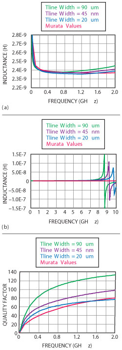
Figure 6 Inductance (a), self resonance (b) and Q-value (c) for three different 2.7 nH inductor designs using the Silex Met-Via 90 TSV process compared to commercial SMD inductors.
Test structures for evaluating the magnetic properties of the novel magnetic composite at RF frequencies were designed and fabricated with a cross-section of the microstrip transmission line test structures shown in Figure 7. From the measured S-parameters, the frequency-dependent characteristic impedance and propagation constant are derived and used to calculate the inductance and capacitance per unit length. Figure 8 shows the inductance enhancement factor for the NiFe/AlN multilayer composite line relative to an SiO2 reference line, achieving an enhancement factor of 4.0 at 1 GHz. The frequency dependent effective relative permeability of the NiFe/AlN multilayer composite material (see Figure 9) is extracted from the measurements by parameter matching of an Ansoft HFSS simulation model to the measured inductance per unit length for all individual frequency points, with the simulation model verified and matched by reference line measurements. An effective permeability of 28 is achieved at 1 GHz, and the ferromagnetic resonance exceeds 3.7 GHz. The permittivity of the composite material is also determined by special dielectric test structures to an effective permittivity of 25. The procedure was verified by measuring known SiO2 reference structures.
The multilayer NiFe/AlN composite material enables an increase in ferromagnetic resonance by a factor of 7.1 as compared to previous work for a homogeneous NiFe film with the same total thickness,7 and thus pushes the usability of commercially manufacturable NiFe films beyond 1 GHz (permeability cutoff at 3.7 GHz). To the authors’ knowledge, an effective permeability of 28 at 1 GHz for on-chip NiFe layers is the highest yet reported.
To illustrate the effect of magnetic core integrated in inductor devices, modeling of a 7.5 nH inductor was done using a CST Microwave Studio simulation model with and without the magnetic core in the 3D inductor geometry. As seen in Figure 10, the SFR is drastically improved using a magnetic core even when assuming a relative low effective µr of 10 for the thick magnetic core material. Simulations have shown that such magnetic materials in connection with 3D-TSV inductors result in an inductance enhancement of up to a factor of 5 at GHz frequencies for the same inductor area, or the same inductance can be achieved at 9 times smaller area and cost.
Future Research and Commercialization
The EPAMO project’s focus extends beyond developing 3D RF inductor technology to encompass complete adaptive antenna front ends. Toward this goal, parallel work is ongoing at Silex for PZT-based MIM capacitors for IPD and energy harvesting applications, and thin film resistors for applications requiring fully integrated R, L and C functions in the IPD as well.
Silex and KTH are also collaborating on separate programs in the areas of advanced polymers for improved TSV and 3D RF-IPD inductor performance. KTH is modeling and designing various RF MEMS devices fabricated by Silex, as well as new research programs on THz microwave components and subsystems.
Acknowledgments
For the work on ferromagnetics, the authors acknowledge process development support from Oerlikon Systems, in particular Harmut Rohrmann, and by Vincent Ip and Katarina Rook of Veeco Instruments, as well as the financial support of VINNOVA under “mag-MEMS” Forska och Väx grant agreement no. 2012-00515. The authors are grateful to Umer Shah at KTH-MST for his simulation, modeling and RF measurement work. For the work on RF TSV and IPD inductors, part of the Silex development was accomplished with support from the European Union [ENIAC JU grant no. 270692-2]. National Swedish funding is provided in part by VINNOVA, the Swedish Governmental Agency for Innovation Systems. National Finnish and Dutch funding is provided by TEKES. The views expressed in this paper are not intended as an endorsement by the funding agencies or the EPAMO consortium.
The authors wish to acknowledge Okmetic Oyj, Finland for providing specially engineered high resistivity silicon 8" wafers to Silex within the
EPAMO consortium. Continued support from all partners within the EPAMO is greatly appreciated. The Silex team acknowledges the Fraunhofer Institute in Germany for assisting in cross-section preparation of the TSV samples; the RF lab of VTT, TNO and EPCOS Netherlands for careful RF characterization of the devices manufactured by Silex; and finally, a special thanks to all the engineers and operators at Silex Sweden who contributed to this research.
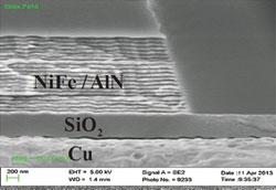
Figure 7 SEM of NiFe/AlN fabricated device.
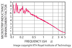
Figure 8 Measured inductance enhancement factor vs. frequency, of microstrip test structures with ferromagnetic NiFe/AlN multilayer composite, relative to an SiO2 reference line.
The following trademarks belong to SILEX Microsystems:
SILEX Microsystems®, Zero-Crosstalk™, TSI™, Sil-Via®, Met-Via®, WL-MSP™, MEMS TO MARKET FASTER™. Met-Via uses XiVia™technology licensed from ÅAC Microtec.
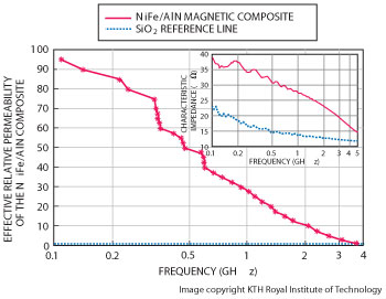
Figure 9 Effective relative permeability of the ferromagnetic NiFe/AlN multilayer composite relative to an SiO2 reference line.
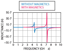
Figure 10 Effect of magnetic materials in TSV based 3D inductors using Ansoft HFSS simulation model.
References
- Xiaoyu Mi and Satoshi Ueda, “Integrated Passives for High-Frequency Applications,” Advanced Microwave Circuits and Systems, Vitaliy Zhurbenko (Ed.), ISBN: 978-953-307-087-2, InTech, DOI: 10.5772/8418, 2010. Available from: www.intechopen.com/books/advanced-microwave-circuits-and-systems/integrated-passives-for-high-frequency-applications.
- www.murata.com/new/news_release/2013/0307/index.html
- ENIAC JU grant no. 270692-2; see Acknowledgments for more information.
- T. Ebefors, J. Fredlund, D. Perttu, R. van Dijk, L. Cifola, M. Kaunisto, P. Rantakari and V. Vähä-Heikkilä, “The Development and Evaluation of RF TSV for 3D IPD Applications,” Extended Abstract - IEEE International 3D Systems Integration Conference (3DIC) Proceedings, October 2013.
- Murata P-SPICE models of inductor LQW15AN2N7C00 are available at www.murata.com/products/design_support/lib/index.html#tab.
- M. Glickman, T. Niblock, J. Harrison, I. Goldberg, P. Tseng and J.W. Judy, “High Permeability Permalloy for MEMS,” Proceedings of the Solid-State Sensors, Actuators and Microsystems Workshop, 2010.
- D.S. Gardner, G. Schrom, F. Paillet, B. Jamieson, T. Karnik and S. Borkar, “Review of On-Chip Inductor Structures With Magnetic Films,” IEEE Transactions on Magnetics, Vol. 45, No