
This direct detection W-Band radiometer front end module for real-time imaging employs a monolithic microwave integrated circuit (MMIC) low noise amplifier (LNA), a highly sensitive detector and a video amplifier. The detector has a responsivity of 1000 mV/mW over a 21 GHz bandwidth. The compact module (measuring 13 × 20 × 56 mm) achieves a temperature sensitivity of 0.83 K with an integration time of 2.3 ms over a 22 GHz bandwidth. It is a candidate for large imaging array applications.
Millimeter-wave (MMW) imaging research and system design for remote sensing has gained much interest in recent years. Compared to active imaging systems, passive imagers have simpler and lower-cost hardware architectures and can detect contraband (for example), often with good fidelity and free of speckle or interference effects.1 W-Band has important applications in passive millimeter-wave (PMMW) imaging under poor atmospheric conditions such as fog2 and dust which generally limit the performance of visible or infrared sensors.
In 1997, Northrop Grumman Corp. developed a direct detection, 1040 channel PMMW imaging receiver array.1 Each channel contained PHEMT LNAs, on-chip switches and a detector diode. It worked at 89 GHz center frequency with a bandwidth of 10 GHz, a temperature sensitivity of 2 K, and a 30 Hz display rate. In 2009, a single channel receiver for PMMW imaging was developed3 with a bandwidth of 17 GHz (85 to 102 GHz) and temperature sensitivity of 1.5 K. In 2010, a direct-detection RFIC for W-Band PMMW imaging was reported.4 It achieved a bandwidth of 20 GHz (83 to 103 GHz) with a temperature sensitivity of 0.69 K. These developments, however, were either physically large,3 or were one of a kind.1,4
In this article, we describe the design of a compact wideband W-Band radiometer front end module with high sensitivity and a 22 GHz bandwidth for real-time PMMW imaging using commercially available components. Due to the lack of on-chip measurement capabilities, separate LNA and detector modules with waveguide interfaces are assembled for design verification. Much work has been done to expand the bandwidth for a higher sensitivity.
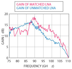
Figure 1 Measured gain comparison of a matched and unmatched LNA.
FRONT END DESIGN
Millimeter wave energy can be rectified directly producing a proportional DC voltage (square law detection), or downconverted to a lower intermediate frequency before detection. For large real-time imaging radiometer arrays and for applications where there is no special requirement for spectroscopic resolution, reduced hardware size, mass and complexity takes precedence over other considerations. For these applications, direct detection is usually a better choice. The temperature sensitivity for a total-power radiometer is given by
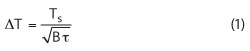
where ΔT is the temperature sensitivity, B is the RF bandwidth, τis the integration time and Tsis the system noise temperature.5 Because requirements for real-time imaging places limits on integration time, increased sensitivity must be achieved through broadening the front end bandwidth.
LNA
An amplifier with low noise, high gain and wide bandwidth at the first stages of the radiometer front end can lower system noise. Even though this design is based on the use of commercial MMIC chips, performance is optimized through the use of multiple bond wires for low impedance, and a broadband external matching network. An antipodal finline transition provides a broadband transition from waveguide to microstrip. A complete LNA module with a standard W-Band flange interface was designed. The LNA’s output impedance matching circuit was optimized and the LNA designed using Ansoft HFSS and Ansoft Designer.
The performance of two LNAs (one matched and one unmatched) is compared in Figure 1. Through appropriate impedance matching, the gain of this single stage LNA is improved by approximately 1 to 7 dB in the upper half of the band, so that the bandwidth, at 10 dB gain, is broadened by about 7 GHz.
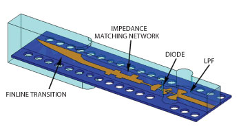
Figure 2 HFSS model of the W-Band planar detector.
Detector
The detector module includes a standard waveguide input flange to interface with the LNA. It consists of a waveguide-to-microstrip transition, impedance matching network, detector diode and output low pass filter (LPF). The design goal was to achieve both wide bandwidth and high sensitivity. An LPF is necessary to extract the quasi-DC information from other abundant spectral components at the output of the detector diode. We selected a structure based on a stepped-impedance of three orders. A radial stub in place of the traditional uniform width transmission line stub broadens the bandwidth of the frequency response and makes the whole circuit more compact. The system bandwidth is maximized when the mismatch over the operating band of the LNA and detector is minimized.6 The center frequency of the detector is set to 89 GHz, in alignment with the LNA. The HFSS physical model of the detector is shown in Figure 2.
The return loss (reflection coefficient), voltage sensitivity (or responsivity) and tangential signal sensitivity (TSS) are the main figures of merit. The measured reflection coefficient is compared with simulated results in Figure 3. There is good agreement, not only at the center frequency and the two adjacent zeroes (85 and 95 GHz), but also at zeros near 100 and 105 GHz at the high end of the frequency band. The measured values, however, are greater by 5 dB or more than the simulated results below 100 GHz and lower by several dB at higher frequencies. This may be due to circuit discontinuities where the detector diode interfaces with the impedance matching network and the LPF. At the highest frequencies, the effects of parasitic capacitance in the simulation become worse, and some potential higher order modes due to the construction of the model may adversely affect the accuracy of simulation.
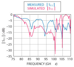
Figure 3 Comparison of the detector simulated and measured | S11 |.
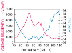
Figure 4 Voltage sensitivity and TSS of the detector.
Responsivity measures the ratio of output voltage to input millimeter wave power and is expected to remain constant in the square law region which is the normal operating range of the detector. Up to 1000 mV/mW responsivity over 78 to 99.5 GHz is measured, with a peak value more than 5200 mV/mW at 86 GHz (see Figure 4).
A tangential signal sensitivity (TSS) measurement is most commonly performed to estimate noise equivalent power (NEP). NEP is the lower limit of the detectable power. TSS is defined as a signal pulse whose bottom level coincides with the top level of the noise on either side of the pulse. The detector’s NEP is related to TSS by
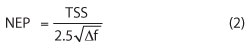
where f is the video bandwidth of the video amplifier following the detector.7 A pulse train with a pulse width of 30 ms and a period of 60 ms simulates the source, and the bandwidth of the video amplifier is approximately 70 Hz. Figure 4 shows that the TSS of the detector is better than –58 dBm over the band from 79 to 100 GHz. The minimum value reaches –64 dBm at several frequency points. According to equation 2, the NEP of the detector is lower than 76 pW√Hz.
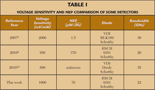
Table 1 lists the performance of several detectors reported in recent years. Except for NEP, which is mainly limited by the detector diode itself, this detector’s performance is comparable to that of Virginia Diode Inc.’s advanced products, which satisfies requirements for high sensitivity and broad bandwidth. Because it is made with commercially available components at a relatively low cost, it is a very competitive candidate for large array applications.
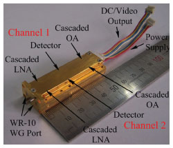
Figure 5 Compact dual-channel front end module.
Module Integration
Based on separate evaluation of the millimeter wave components, the integrated front end module was designed and is shown in Figure 5. The MMW circuits of each channel are separated in different chambers to minimize mutual interference. Two operational amplifier (OA) stages, along with RC integration circuits, constitute the main structure of the video amplifier section. A differential OA is chosen as the second stage, converting the single ended input to a balanced output in order to suppress common mode interference. The link gain is adjusted so that the output voltage level is placed in the required range for A/D conversion. Power supply components are located on the bottom side of the module.
It has been previously demonstrated that in the presence of a highly directional antenna, only when the sampling rate slows down from 0.5 wavelengths (Nyquist sampling density) to larger than 3.13 wavelengths per sample, is there a perceived reduction of target sharpness.11Therefore, the spacing between adjacent module channels is chosen as 9.96 mm to make the module design easier and decrease the number of elements of the array for a given aperture. The module has regular shape and is no larger than 13× 20 × 56 mm. This compact size makes it applicable for miniaturization and modularization.
MEASUREMENTS
Frequency Response
Since the interface of the two waveguide ports is not a standard W-Band flange, a specially designed connector is introduced to provide matched interface for measurement. The input power is set to produce a maximum power without driving the video amplifier into saturation. This is about –72.5 dBm. The measured frequency response (see Figure 6) shows that the radiometer front end module has a response above 650 mV in over a bandwidth of at least 22 GHz and a peak value appearing near 89 GHz. This verifies the design predictions.
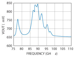
Figure 6 Frequency response of the radiometer front end module.
Calibration
A set of W-Band standard hot-cold calibration sources is introduced to measure the temperature sensitivity based on the two-point calibration equation,12
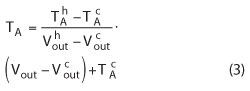
where TAh/TAc corresponds to the antenna temperature of the hot/cold calibration source, respectively, (80°C/6°C) and Vouth / Voutc represents the output voltage of the front end (–186 mV/–400.59 mV) over integration time τ(2.3 ms, the same as that in the measurement of the individual detector module). Then the deduced calibration equation (V in mV and T in K) is obtained as:
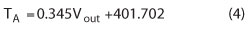
With the root mean square (RMS) voltage of the observed data equal to 2.4 mV, the calculated sensitivity of the radiometer is about 0.83 K. The renormalized system sensitivity to integration time is about 0.04 K/√Hz.
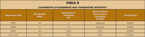
Table 2 lists the recently reported performance of several W-Band direct detection type radiometers for comparison. Due to the compact structure and on-chip interconnects between the LNA and detector and other circuits integrated in a single chip, carefully designed MMICs often tend to have intrinsically lower noise and smaller internal insertion loss than Hybrid Microwave Integrated Circuit (HMIC) counterparts. This design, however, has achieved comparable performance and some improvements in bandwidth and sensitivity at relatively low cost2based on the use of commercially available components.
Conclusion
A compact wideband W-Band radiometer front end module for real-time imaging is designed, demonstrating at least 22 GHz bandwidth and a sensitivity of 0.04 K/√Hz. Subsequent single channel scanned imaging experiments have been conducted, showing that the W-Band radiometer system can produce a passive planar image, thus validating its practical value in large arrays for PMMW imaging. Further performance improvements are possible through refinements of the diode model.13
Acknowledgments
This work is supported by the State Key Program of National Natural Science Foundation of China (No. 60632020) and the National High Technology Research and Development Program of China (863 Program, NO.2007AA061903).
References
- L. Yujiri et al., “Passive Millimeter-Wave Camera,” Proceedings of the SPIE Conference on Passive Millimeter-Wave Imaging Technology, Vol. 3064, April 1997, pp. 15-22.
- H.J. Liebe, “An Updated Model for Millimeter Wave Propagation in Moist Air,” Radio Science, Vol. 20, No. 5, May 1985, pp. 1069-1089.
- M. Jung, Y. Chang, S. Kim, W.G. Kim and Y.H. Kim, “Development of Passive Millimeter Wave Imaging System at W-Band,” 34th International Conference on Infrared, Millimeter and Terahertz Waves, September 2009, pp. 1-2.
- J.W. May and G.M. Rebeiz, “Design and Characterization of W-Band SiGe RFICs for Passive Millimeter-Wave Imaging,” IEEE Transactions on Microwave Theory and Techniques, Vol. 58, No. 5, May 2010, pp. 1420-1430.
- F. Ulaby, R. Moore and A. Fung, Microwave Remote Sensing: Active and Passive, Artech House, Norwood, MA, 1991.
- Y.B. Jiao, Y.H. Zhang and Y. Fan, “Research on Modeling of W-Band Wide-Band Total Power Radiometer Channel,” Journal of Electromagnetic Waves and Applications, Vol. 23, No. 8-9, 2009, pp. 1049-1058.
- A.M. Cowley and H.O. Sorensen, “Quantitative Comparison of Solid-State Microwave Detectors,” IEEE Transactions on Microwave Theory and Techniques, Vol. 14, No. 12, December 1966, pp. 588-602.
- J.L. Hesler and T.W. Crowe, “Responsivity and Noise Measurements of Zero-Bias Schottky Diode Detectors,” Proceedings of the 18th International Symposium on Space Terahertz Technology, March 2007, pp. 88-92.
- L.L. Xie, Y.H. Zhang, Y. Fan, C.H. Xu and Y.B. Jiao, “A W-Band Detector With High Tangential Signal Sensitivity and Voltage Sensitivity,” Proceedings of the International Conference on Microwave and Millimeter Wave Technology, May 2010, pp. 528-531.
- T. Baek et al., “A 94 GHz Receiver Front End for Passive Millimeter-Wave Imaging,” Proceedings of the 7th European Radar Conference, October 2010, pp. 348-351.
- L. Zhang, Y. Hao, C.G. Parini and J. Dupuy, “An Investigation of Antenna Element Spacing on the Quality of Millimetre Wave Imaging,” Proceedings of the IEEE Antennas and Propagation Society International Symposium, July 2008, pp. 1-4.
- M.S. Herman and G.A. Poe, “Sensitivity of the Total Power Radiometer with Periodic Absolute Calibration,” IEEE Transactions on Microwave Theory and Techniques, Vol. 29, No. 1, January 1981, pp. 32-40.
- J. Liu, H. Morales, T. Weller, L. Dunleavy and G. Schoenthal, “Ultra-Wideband Nonlinear Modeling of W-Band Schottky Diodes,” Microwave Journal, Vol. 55, No. 9, September 2012, pp. 144-148