
This article provides an overview of radio frequency (RF) delivery systems including RF generators and matching networks, which are one of the most critical surrounding components of the plasma chamber in wafer processing. Subcomponents of the RF generators including RF power amplifiers, combiners, couplers and filters are presented. Radio frequency power levels, frequency allocation and operational modes are studied. Matching networks and RF amplifier topologies used in RF delivery systems are also discussed.
Semiconductor wafer processing is used to manufacture integrated circuits (IC) that are components in the most sophisticated electronic products that are used in everyday life. In fact, the state of technology in semiconductor wafer processing is a driving force for the invention and development of new electronic devices due to enhanced features of the manufactured ICs. Devices or ICs are formed, for the most part, on the typical silicon wafer surface where 200 to 300 identical devices are formed on each wafer. The area on the wafer occupied by the discrete device or IC is called a chip or die. Bare and patterned silicon wafers are illustrated in Figure 1. Fabrication processes of ICs involve many steps including layering, patterning, doping and heat treatment.1-4 Layers consist of insulators, semiconductors or conductors. Layers can be added by deposition that can be implemented by chemical vapor deposition (CVD)5 or physical vapor deposition (PVD).6 The main categories of PVD processing are classified as evaporation and sputtering.7 The process of etching is also used in manufacturing ICs mainly to remove the unwanted material from the wafer. There is conductor etching and dielectric etching depending on the application. All the processes described take place when the wafer is placed inside a chamber which is also commonly called as a process or plasma chamber.
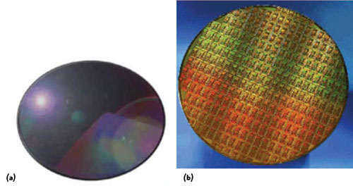
Figure 1 Bare (a) and patterned silicon wafers (b).
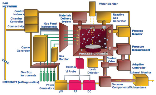
Figure 2 Illustration of process chamber with surrounding components for semiconductor wafer processing.
The typical illustration of the process chamber for semiconductor wafer processing with its surrounding components is illustrated in Figure 2. Inside the process chamber, partially ionized gas with a combination of free electrons, ions, radicals and neutral species called plasma is used to accomplish the processes described including deposition, etching and cleaning. The generation and sustaining of a plasma inside the process chamber is possible with the RF energy. RF waves are used to provide energy to target materials (typically insulators) and bias substrates in processes where plasma is required. As a result, the level of RF energy, RF signal purity, RF interface impedance, application frequency and RF wave shape applied carry great importance to accomplish selective wafer processing including uniformity, etch rate, anisotropy, etc. RF energy is applied via RF generators that are connected to process chambers with matching networks. Impedance and power measurement devices such as a V/I probe8 can be included in the system to give users the ability to monitor several important parameters such as the level of RF energy, chamber impedance and the corresponding RF frequency.
RF Delivery System
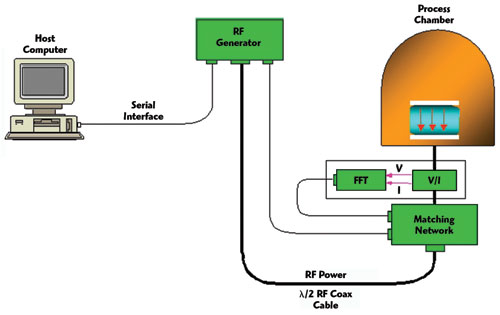
Figure 3 Typical RF delivery system for the process chamber.
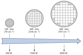
Figure 4 Wafer size transitions and corresponding cost per watt.
Typical RF delivery systems consist of an RF generator, matching network, impedance and power measurement device, which are illustrated in Figure 3. In the system shown, RF power is provided at the desired power level and the operational frequency is set by the user via a host computer that communicates with the generator using series type communication such as RS-232 or RS-485. RF generator power output is connected to an automated matching network using half a wavelength RF coax cable at the operational frequency. The communication between RF generator and matching network is usually established with optical communication for immunity to electromagnetic interference. Output of the matching network is connected to an impedance and power monitoring device such as a V/I probe before it is connected to the plasma chamber as shown in Figure 3. The V/I probe captures the forward and reflected voltage, current and associated phase information and feeds them to the matching network to find the tune point to match the generator output impedance to the plasma impedance so that maximum power transfer is accomplished.
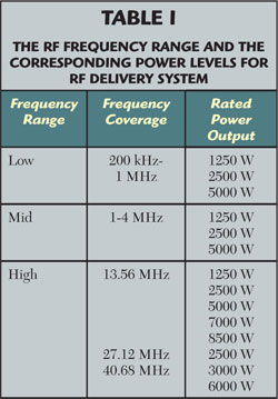
After the 1990s, use of RF energy became necessary to achieve sophisticated structures for IC manufacturing in processes such as high density CVD, PVD and plasma enhanced physical vapor deposition (PECVD) and etching. Wafer size transitions have occurred because of the overall cost benefits resulting from the larger number of dice per wafer, thereby using the same number of process steps to produce more dice. Wafer size transitions and corresponding cost per watt are shown in Figure 4. The most common frequencies for providing RF energy range from 200 kHz to 40.68 MHz with power levels from 1250 to 6000 W as shown in the Table 1 for processes such as sputtering of metallic/conductive or insulating and semi-conductive materials onto substrate, biasing of substrate during deposition and etching. RF generators and matching networks are designed to meet the power requirements in Table 1 at the frequencies given. It is also possible to obtain higher power levels from RF generators using RF amplifiers in modular structure by paralleling them. In the recent years, it also became apparent for original equipment manufacturers (OEM) to use RF pulsing in conjunction with continuous wave to enhance their manufacturing process.
RF Generators
A typical RF generator architecture used in semiconductor wafer processing is illustrated in Figure 5. In the design and implementation of RF generators, it is common practice to design PA modules for lower power levels and obtain higher power levels by paralleling them via combiner as shown in Figure 5. The output of combined RF power then goes through the filter which eliminates higher order harmonics. RF generators have an internal directional coupler located right before an RF signal is sent to the matching network for sensing forward and reverse reflected powers and providing feedback signal to the system controller to maintain stability. The stability of the generator is essential to meet the strict requirements to have selective wafer processing. The RF signal purity in semiconductor wafer processing is so critical that manufacturers demand RF generators to provide RF signal output to have spurious and harmonics levels lower than –30 dB for any load condition.
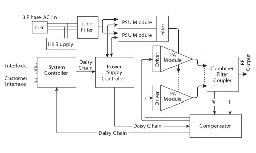
Figure 5 Typical RF generator architecture used in wafer processing.
RF power amplifier topologies used in wafer processing also range from linear to nonlinear amplifiers such as switch mode amplifiers. Commonly used linear amplifiers are usually implemented in Class AB mode whereas nonlinear amplifiers are implemented in Class C, D or E modes. The biggest differences between linear and nonlinear type switch-mode amplifiers are their efficiency and the signal purity. As a result, there is a trade off when one of the topologies is preferred. For instance, when a linear mode amplifier topology is used, although RF signal purity is inherently good, it is a cost driving factor to obtain a higher level of output power due to lower efficiency. Several linear type PA modules have to be combined to obtain the desired power level. When a switch-mode amplifier is used, it is possible to obtain higher power levels with fewer PA modules, however, designers have to implement filter sections to purify the signal that exists at the output of the amplifier due to its nonlinear characteristics. The operational principle of linear and nonlinear amplifier modes are illustrated in Figure 6 when two amplifiers are working as push-pull amplifiers.9 Removing the bias and adjusting the low frequency stability network by opening the switch S and slightly modifying input impedance matching network and the load line network in Figure 6 changes the operational mode from linear to nonlinear mode.
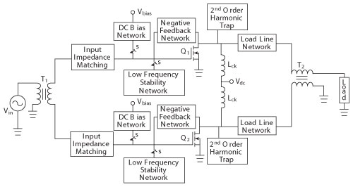
Figure 6 Linear and nonlinear RF amplifier topology implemented as push-pull amplifier.9
In recent years, OEMs have also required RF generators to have pulsing capability in addition to all the requirements in continuous mode including signal purity, power levels, dual frequency capability, bandwidth, etc. The RF pulsing capability of amplifiers depends on the amplifier topology used. There are several factors that affect the pulsing capability of the amplifier. These factors for ON/OFF and 2-Level Pulsing are shown in Figure 7 for linear and switch-mode amplifiers. The typical waveforms for ON/OFF pulsing using linear mode Class AB and switch mode Class E amplifiers are shown in Figure 8.
RF Matching Networks
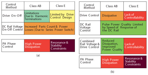
Figure 7 Pulsing capability of linear and switch-mode amplifiers in ON/OFF mode (a) and 2-Level Pulsing Model (b).
Automated RF matching networks are critical components that provide the matched impedance interface to RF generator even when there is a change in the plasma impedance, as shown in Figure 3. In fact, the plasma impedance that is formed during the processes can vary from very low impedance to very high impedance in a short time period due to the dynamic structure of the plasma. As a result, matching networks should be able to respond to the sudden changes occurring in the process chamber. One of the ways matching networks accomplish a tune point is to follow the changes in the impedance of the plasma using a device called Phase/Magnitude detector. The Phase/Magnitude detector captures the magnitude of the RF voltage and current and phase information to determine the impedance. Once the calculated impedance information is fed back to the controller system, the control system determines the capacitance needed to accomplish the tune point with fuzzy logic. Most of the time two vacuum variable capacitors are used inside matching networks. The reason for the use of vacuum variable capacitors is due to the fact that they have very high voltage breakdown values. The vacuum variable capacitors are connected to the stepper motors which control the position of the plate inside the capacitor that changes its capacitance value. The capacitor position information to achieve the tune point is sent to the stepper motors via a controller system of the matching network. Continuous closed loop operation in the matching network minimizes the error in the phase and the magnitude information that is acquired by the Phase/Magnitude detector and matching is accomplished this way.
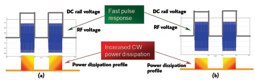
Figure 8 ON/OFF Pulsing illustration of linear (a) and switch mode (b) RF amplifiers.
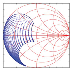
Figure 9 Tuning range of MKS Instruments' matching network, MWH-100.
Matching networks use L or PI type topology depending on the specific process and operational frequency. Approximate plasma impedance is usually provided to matching network manufacturers for implementation of their design. Matching networks can only accomplish matching if the impedance of the plasma falls within the tune range of the matching network. For instance, the tune range of MKS Instruments’ 13.56 MHz matching network MWH-100 is shown in Figure 9.10 The architecture of commonly used matching networks is illustrated in Figure 10 where M1 and M2 represent the stepper motors whereas C1 and C2 represents vacuum variable capacitors.
Conclusion
In this article, the RF delivery system with its critical components including RF generators and matching networks for semiconductor wafer processing have been analyzed in detail. The architectures used in practice to design and implement RF generators and matching networks are given. The processes where RF delivery system are used, operational frequencies and corresponding power levels are presented. RF amplifier topologies, a comparison of linear versus nonlinear amplifiers for continuous wave and pulsing modes have been discussed. Matching networks, network topologies and a method to control the tuning mechanism have been detailed. The information regarding wafer size changes and their impacts on cost and technology are also summarized.
References
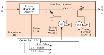
Figure 10 The architecture of the matching network used in practice.
- H. Geng, Semiconductor Manufacturing Handbook, McGraw-Hill Professional, 1st Edition, April 27, 2005.
- S.M. Sze, VLSI Technology, Second Edition, McGraw-Hill Inc., 1988.
- S. Wolf, Microchip Manufacturing, Lattice Press, 2004.
- Y. Nishi and R. Doering, Handbook of Semiconductor Manufacturing Technology, CRC Press; 2nd Edition, July 9, 2007.
- D.M. Dobkin and M.K. Zuraw, Principles of Chemical Vapor Deposition, Springer, 1st Edition, April 1, 2003.
- D.M. Mattox, Handbook of Physical Vapor Deposition (PVD) Processing, William Andrew, 2nd Edition, May 19, 2010.
- A.Z. Moshfegh, “PVD Growth Method: Physics and Technology,” Proceedingsof the International Workshop on Physics and Technology of Thin Films, March 2003.
- MKS Instruments V/I Probe Datasheet: www.johnmorris.com.au/files/product/attachments/5846/214660_opt4.pdf.
- A. Eroglu, “RF Power Amplifiers for Pulsing Applications,” International Review on Modeling and Simulations, Vol. 3, No. 3, pp. 423-427, June 2010.
- MKS Instruments Matching Network Datasheet: www.mksinst.com/docs/UR/eni-MWH100-SmithChart.aspx.