
RFIC Receiver Technology for Digital Mobile Phones
Chris O’Connor
TriQuint Semiconductor
Hillsboro, OR
The Cellular Telephone Industry Association (CTIA) reported recently that 17 percent of the US population now uses wireless telephones. Amazingly, more than 44 million subscribers were on record as of December 31, 1996, with new subscribers signing up at the rate of approximately 28 thousand per day. Cellular telephones are now accepted widely and the market is growing faster than any consumer product in history. Most users have become accustomed to the convenience and utility of mobile phone service. However, many customers are interested in improved voice quality and additional features, such as short text message paging. Service providers and phone manufacturers have responded by developing new digital wireless standards and products.
Several digital mobile phone standards have been deployed around the world, including the Global System for Mobile communications (GSM) worldwide, code-division multiple access (CDMA) (IS-98) in the US and Asia, time-division multiple access (TDMA) (IS-136) in North and South America, and personal digital cellular (PDC) (RCR-27) in Japan. These standards have been allocated spectrum at cellular frequencies (800 to 1000 MHz) and personal communications service (PCS) frequencies (1700 to 2000 MHz). In each instance, the digital technology delivers improvements over the existing analog system in terms of system user capacity, data handling, convenience features, messaging and, ultimately, transmission quality. However, these improvements come at the expense of a more complex, performance-critical system. The radio system components used in the digital phone must provide improved linearity and noise performance as well as significant digital signal processing (DSP) for demodulation, encoding/decoding and control.
Changing Demands on Handset Manufacturers
Interestingly, wireless industry surveys of customers have revealed that their main concern is the need for improvement in transmission quality and a decrease in disconnections (dropped calls). Carriers and phone manufacturers have discovered that in real-world use the mobile phone is subjected to more interferers than specified by the standard, due primarily to an increasingly crowded radio environment.
In addition, customers are requesting longer standby and talk times. They want batteries to last longer so that charging or replacement is less frequent. A week or more in standby mode without needing to recharge the batteries is ideal and is especially desirable when paging features are available. On the other hand, talk time of almost a day is viewed as excellent.
Finally, the increasingly competitive wireless commercial environment has made it necessary for service providers to pay for all or part of the cost of the mobile phone. Initially, service providers were willing to pay several hundred dollars for a new digital handset and subsidize the customer in exchange for long-term service commitments. However, as the new digital services compete against traditional analog cellular, service commitments are decreasing. Therefore, a primary cost of customer acquisition, the purchase price of the mobile phones, inevitably must decrease for the service provider. This cost reduction translates directly into a required decrease in manufacturing costs and, ultimately, component costs, which account for most of the manufacturing cost of a mobile telephone.
Digital Mobile Phone System Standards for Signal Reception
Mobile phones are type-approval tested by the wireless industry regulatory agencies (such as the CTIA) to verify conformance to the standards. Each system standard specifies a set of operating parameters and modes that must be met in order for the phone to be certified as complying with the standard and, therefore, capable of functioning properly with a service provider’s network. For signal reception, the system standards require that the mobile phone provide a particular signal sensitivity, intermodulation distortion rejection and signal-handling range. Table 1 lists the major receiver specifications vs. the various digital mobile phone standards. It is critical that these parameters are met to maintain an acceptably low bit error rate (BER) or frame error rate (FER) during the signal reception.
|
Table 1 - Receiver Requirements vs. Cellular/PCS Digital Mobile Phone Standards | ||||
|
|
IS-136 |
IS-98 |
GSM |
PDC |
|
RX frequency (MHz) |
|
|
|
|
|
cellular |
869 to 894 |
869 to 894 |
890 to 915 |
810 to 828, 870 to 885 |
|
PCS |
1930 to 1990 |
1930 to 1990 |
1930 to 1990 |
1477 to 1501 |
|
Channel bandwidth (kHz) |
30 |
1230 |
200 |
25 |
|
Modulation |
¶/4 QPSK |
QPSK |
GMSK |
¶/4 QPSK |
|
Sensitivity (dBm) |
-110 |
-104 |
-99 |
-109 |
|
IMD rejection * (dBm) |
|
|
|
|
|
Psig |
-107 |
-101 |
-99 |
-106 |
|
Pint |
-42 |
-43 |
-49 |
-49 |
|
BER/FER limit (%) |
3.0 |
0.5 |
2.0 |
1.0 |
|
C/N & C/I ** (dB) |
11 |
0+ |
9 |
12 |
|
|
|
|
|
|
* Desired RF signal and two-tone interference levels for which the mobile phone must maintain less than or equal to the listed BER or FER
** Typical values for receiver C/N and C/I required by mobile phone demodulators to maintain less than or equal to the listed BER or FER; approximately 2 dB greater than theoretical
+ Does not include CDMA processing gain
Any degradation in sensitivity and intermodulation distortion rejection may drop the radio system carrier-to-noise (C/N) or carrier-to-interference (C/I) ratios below the required minimum and during weak signal reception result in a rapidly increasing BER. Figure 1 shows a typical graph of BER vs. C/(N + I). 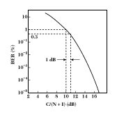 Unlike analog systems in which the degradation causes a gradual decrease in reception quality, digital communications systems (DCS) shut down when the BER gets too high during reception (the data/voice output is cut off abruptly by the DSP part of the system). Normally, the system can tolerate a cutoff for short periods and still maintain the call connection. However, if the excessively high BER occurs for too long, the call connection is dropped.
Therefore, in a DCS, high reception quality depends on maintaining a low BER. A direct relationship exists between BER and the C/(N + I) ratio, which is determined by the modulation scheme and fundamental communication signal theory error probabilities. It is evident from the BER vs. C/(N + I) relationship how quickly BER changes following a change of a couple decibels in C/(N + I). Typically, in most digital mobile phone standards the maximum allowable BER is one to three percent. A minimum C/(N + I) is required to remain below the particular maximum BER permitted by the system standard.
It is the RF designer’s responsibility to take the system sensitivity and intermodulation distortion specifications, combined with the required minimum C/N and C/I of the system’s demodulator circuitry, and compute the level of noise and the distortion performance required from the receiver components. Typically, both the service provider and the phone manufacturer insist on adding a few decibels of margin to ensure that the transmission integrity is always preserved given the sensitive nature of BER vs. C/(N + I). The result is a very demanding requirement on the noise and distortion performance of the receiver front end. Overall, the noise and distortion performance are controlled by the receiver front end, the low noise amplifier (LNA)/mixer and the preceding filter. The precise cascaded noise figure and input third-order intercept (IIP3) calculations are beyond the scope of this article, but the LNA/mixer must provide a relatively low noise figure and high input intercept.
Impact on the Radio System Design
Improvements in transmission quality and the reduction of dropped calls have a direct impact on the RF performance needed in the radio system. However, good receiver RF performance cannot be pursued at any cost. The RF designer is constrained by strict requirements for low current operation to help maximize standby time. Low current operation is directly at odds with higher RF performance. Generally, better RF performance is met by operating the telephone’s circuitry at higher currents, which is not an acceptable option. This limitation presents a serious challenge to the RF design engineer that must be solved.
Despite the required performance optimization, the resultant receiver cost must be low enough to support the consumer product pricing model.  The cost of the phones is under continuous downward pressure from the service providers and manufacturers who are trying to gain market share. Figure 2 shows the relative cost of digital mobile phone manufacturing vs. time. The chosen receiver technology also must be capable of moving down this cost vs. time curve.
IC Technology Options
Most mobile phone manufacturers already have or currently are converting rapidly from discrete transistor receiver designs in their mobile phones to IC receiver designs. Today’s RF designer has several IC technology options to explore as potential solutions to his or her receiver design problem. Among the available technologies are Si bipolar (or BiCMOS), Si MOSFET, GaAs MESFET and GaAs heterojunction bipolar transistor (HBT). Mobile phone manufacturers have assessed the needs in their next-generation products and have surveyed these RFIC technologies. Each technology has its own set of strengths. Generally, trade-offs exist between RF performance, cost and RF integration. The relative trade-offs between RF performance (gain, noise figure and IIP3) and cost are shown in Figure 3 . 
The RF designer of mobile phones is looking for the ideal RFIC receiver solution to provide low noise, high IIP3, low current consumption, high RF integration and low implementation cost. Many have concluded that GaAs MESFET RFICs are an attractive option for the RF functions and come closest to providing the ideal solution. The companies are attracted to the excellent RF performance, small size and competitive cost.
Today, silicon bipolar/BiCMOS and GaAs MESFET technologies dominate the usage of RFIC in mobile phones. Silicon solutions have realized widespread popularity in cordless phones and GSM applications with their high level of integration and low cost chip set approach. On the other hand, GaAs solutions have found wide use in the performance/price-critical applications of TDMA (IS-136), CDMA, personal handyphone and wireless local area networks. The fact that GaAs RFIC technology is a good compromise between excellent RF performance and cost-effective RF integration is leading to even greater use in digital mobile phones. Table 2 lists the major RFIC technologies.
|
Table 2 - RFIC Receiver Technology Comparison | |||||
|
|
Ideal |
MESFET |
RF MOSFET |
Bipolar |
HBT |
|
Noise figure |
low |
low |
high |
moderate |
low |
|
Input IP3 capability |
high |
high |
moderate |
moderate |
high |
|
Current consumption |
low |
low |
moderate |
moderate |
low |
|
Passive component integration |
high |
high |
low |
low |
high |
|
Implementation |
low |
low |
low |
low |
moderate |
GaAs MESFETs
Fundamentally, GaAs MESFET-based RFICs can provide a lower minimum noise figure, higher input intercept capability, better mixer structures and the path to lowest power consumption for a given RF performance. Analysis of silicon bipolar, MOS and GaAs transistors points out the fundamental device limits in noise figure. Mixer noise figure is lower due to better mixer topologies possible with GaAs MESFETs. Typically, the cascade (LNA + filter + mixer) downconverter noise figure is 1 to 2 dB lower and the IIP3 is 1 to 3 dB higher for the GaAs MESFET RFIC than for competing silicon bipolar/BiCMOS solutions. The input intercept also may be significantly higher, when necessary, for applications such as in CDMA systems. In addition, high frequency properties enable low noise figure and high input intercept to be achieved at both cellular and PCS frequencies. Therefore, the technology produces RF solutions that deliver the RF performance necessary for system margin in noise and distortion, which translates directly into better transmission quality and fewer dropped calls.
The high level of integration of passive elements has produced RF designs that occupy significantly less board area than competing technologies. With GaAs receivers, the majority of inductors and capacitors can be integrated on the chip. Only the most critical or large-value matching elements are left off the chip. The RF integration capability squarely addresses the need to reduce size in succeeding generations of mobile phone products. Coupled with smaller, surface-mount plastic packaging, GaAs RFICs are the smallest solutions available today to the radio system designer.
Commercial GaAs MESFET Receivers
Several new receiver IC products have been developed specifically for CDMA (IS-98) and TDMA (IS-136) PCS applications, including two PCS CDMA LNA/mixer ICs and a dual-band TDMA LNA/mixer IC. The overall downconverter performance for three components is listed in Table 3 . The conversation gain results include a 2.5 dB insertion loss filter.
|
Table 3 - PCS LNA/Mixer IC Parameters | ||||
|
|
TQ9225 |
TQ9228 |
TQ9222 |
TQ9222 |
|
|
|
|
low band |
high band |
|
RF frequency (MHz) |
1930 to 1990 |
1930 to 1990 |
869 to 894 |
1930 to 1990 |
|
LO frequency (MHz) |
1710 to 1790 |
2015 to 2075 |
920 to 1040 |
2000 to 2140 |
|
IF (MHz) |
210 to 212 |
84 to 86 |
70 to 140 |
70 to 140 |
|
Gain * (dB) |
28.0 |
27.0 |
17.5 |
17.5 |
|
Noise figure * (dB) |
2.4 |
2.4 |
2.8 |
2.8 |
|
Input IP3 * (dBm) |
-9 |
-9 |
-10 |
-10 |
|
Gain step (dB) |
20 |
20 |
- |
- |
|
Supply voltage (V DC) |
3.0±5% |
3.0±5% |
2.7 to 3.0 |
2.7 to 3.0 |
|
Supply current (mA) |
52 |
52 |
10 |
20 |
* Values given for downconverter RF performance include a 2.5 dB insertion loss image filter between the LNA and mixer
The PCS devices are 3 V RF receiver ICs designed specifically for PCS-band CDMA applications. This performance meets the demanding requirements of IS-98 standard-based products for both portable and fixed wireless applications. The downconverter architecture is split in a manner to maximize LNA dynamic range while maintaining good overall downconverter performance. The RF frequency range covers the entire PCS band for both components. One of the LNA/mixer ICs uses a low side LO frequency range and a 211 MHz IF. The other IC uses a high side LO frequency range and an 85 MHz IF, which permits its use with various manufacturers’ chip sets. The half-IF spurious rejection is greater on the latter IC to permit the use of the lower IFs. Both ICs are packaged in a small 24-pin QSOP-24 surface-mount plastic package and operate from a single 3 V supply voltage compatible with 3.6 V battery phones. A gain select function supports the large-signal mode in IS-98. An LO buffer is included on chip to drive the transmit LO input. A differential output on the IF port offers improved half- IF rejection and better low frequency noise immunity. On-chip matching to 50 W streamlines the design and improves the ease of use greatly.
The TDMA LNA/mixer is a 2.7 V RF receiver IC designed specifically for dual-band TDMA applications. The performance meets the requirements of IS-136 standards for mobile phone products. The RF frequency range covers the entire cellular and PCS frequency bands. The LO frequency range is on the high side and the IF frequency range is 70 to 140 MHz. The low band downconverter architecture provides the higher LNA IIP3 and lower supply current sufficient to support Advanced Mobile Phone Service (AMPS)-mode operation. On the other hand, the high band downconverter architecture, offers greater half- IF spurious rejection to support low IFs (< 120 MHz). A gain select function is also included to provide the large-signal mode to support the full signal range specified in IS-136. The IC also is packaged in a QSOP-24 package, and operates from a single 2.7 to 3 V supply voltage compatible with 3.6 V battery phones. The IC employs on-chip matching to 50 W and the IF outputs can be combined externally through the IF matching networks into a single IF filter connection.
Future Trends in Receiver and RFIC Development
GaAs RFIC receivers continue to appear in numerous mobile phone applications and products, and are delivering the performance and value required by the major digital mobile phone manufacturers. The utility and competitiveness of the technology is proven. However, in spite of these advantages, the performance and value of the GaAs receiver RFICs alone are not sufficient to sustain the long-term advance of mobile phones.
The relentless push by the mobile phone manufacturers for lower cost, smaller form factor and more efficient use of the battery will continue in future generations of phones. The phones of the future will be ultralight credit card-size flip phones that slip easily into a shirt pocket. They will be convenient, affordable and sound great. To achieve these objectives, the phones cannot relinquish any performance. In fact, much improved power consumption efficiency will be needed to support the smaller batteries necessary for these ultra-small phones. Also, the demands by consumers for improved transmission quality and operation in the PCS frequency spectrum are forcing manufacturers to design for slightly greater performance to ensure that call quality is preserved in the crowded cellular and PCS airwaves.
Unit prices will continue their trend downward for mobile phones, but likely will reach a limit of approximately 1.5 times that of present analog mobile phones. Manufacturers will continue to emphasize cost reduction for all components in the mobile phone, including the RF front ends. However, as the decreases become more difficult to sustain, breakthrough changes in the cost/function equation will be required. The only viable method to achieve this goal as well as to reduce size is through advanced integration techniques. This integration is occurring in the DSP baseband, peripheral control, IF/synthesizer and power-management parts of the mobile phone system. However, in the RF front end, only partial integration has taken place and typically uses more than one technology. The key strategy is to integrate all of the RF circuitry in a technology capable of supporting the required RF performance and higher levels of integration.
CONCLUSION
GaAs RFIC technology is already a consensus choice among phone manufacturers for implementing power amplifiers. It has proven equally useful for receiver solutions in digital mobile phones. GaAs RFIC technology is capable of integrating the transmitter and receiver technology on the same chip while maintaining good RF performance and modest cost. It is clear the technology is capable of delivering on the promise of a single-chip RFIC and is an important component technology in the development of digital phone products.