
GaAs MMICs for Changing Base Station Requirements
Hittite Microwave Corp.
Woburn, MA
Today, wireless infrastructure designers are being faced with increasingly challenging design requirements. Cellular base transceiver stations (BTS), or base stations, are becoming smaller, smarter, higher performance, self-contained and lower cost simultaneously.
Early cellular BTS designs, which are still in use today, placed equipment in secured, environmentally controlled buildings at the base of an antenna tower. Engineers had to work with one or more closet-sized cabinets, tame environmental conditions, little limit on power consumption and moderate cost pressure. In contrast, handset designers have long been faced with severe size, weight, power and cost constraints.
Recent advances made in MMIC components to satisfy handset requirements are becoming ever more appropriate for the BTS engineer designing macro, micro and picocell equipment. BTS the size of a shoebox to a briefcase are not uncommon in current-generation equipment designs. Table 1 lists the differences between the old and new cellular BTS designs.
|
Table 1 -- Evolving Cellular Base Station Requirements | ||
|
BTS Characteristics |
Old Requirement |
New Requirement |
|
Technology |
analog |
analog and digital |
|
Frequency band |
800/900 MHz |
800/900 MHz and 1.8/1.9 GHz |
|
Standard |
FDMA or TDMA |
FDMA/TDMA/CDMA/GSM/PDC |
|
Architecture |
macrocell |
macro, mini, micro, pico |
|
Antenna configuration |
omni or three sector |
up to 12 sector, dynamically configured |
|
Environment |
indoor |
indoor and outdoor |
|
Cell site size |
small room at base of antenna tower |
zoning restrictions on large cell sites; wall, roof or poletop mounting desired |
|
PCB power supply |
not limited, positive and negative |
somewhat limited, prefer positive only |
|
|
|
|
GaAs MMIC Components for BTS
Innovative GaAs MMICs have been developed to meet these demanding and dynamic requirements. Monolithic, plastic-packaged devices including multithrow switches with integrated decoder drivers, single positive control voltage-variable attenuators (VVA), double-balanced mixers and frequency doublers enable BTS engineers to improve performance, reduce size and lower cost.
Miniature Multithrow MMIC Switches for Cellular BTS
Multithrow switches are used in cellular BTS for receive-side antenna switching to one or more low noise amplifiers, to combine antenna paths on smart BTS systems for switched filter banks and switched delay lines, and to provide high isolation between differential LO sources. A new line of SPNT MMIC switches that operates from DC to 3 GHz, covering all BTS bands, has been developed. The product line comprises SPDT, SP4T, SP6T and SP8T switches, making it the most complete line of multithrow GaAs MMIC switches on the market today. These switches include on-chip logic decoders and drivers that save components, board area and design time, and offer high third-order intercept (IP3) performance (+40 to +50 dBm). The switches are housed in standard plastic surface-mount technology (SMT) packages, saving cost and space. In addition, the monolithic GaAs MMIC technology used provides consistency and high reliability.
Multithrow switch designs of the past used multiple PIN diodes or hybrid multithrow switches prior to the introduction of GaAs MMIC switches. To achieve an eight-throw configuration, up to 16 diodes and numerous control circuit components were required. Alternatively, cascaded multithrow hybrid switches could also perform the function. These approaches result in numerous control lines and components, reduced isolation due to control line cross talk and a relatively large complex board layout. A more contemporary SP8T approach uses one SPDT and two SP4T GaAs MMIC switches requiring 10 to 18 control lines and associated logic drive circuitry (still not a small and simple approach). This article describes the alternate switching configurations utilized in this new line of SPNT switches. Table 2 lists important specifications of a sampling of the SPDT, SP4T, SP6T and SP8T products. All of the SPNT switches are fabricated using a standard commercial 1 mm enhancement/depletion GaAs MESFET process. All of the switches have guaranteed specifications for operation from –40° to +85°C.
|
Table II -- MMIC Switch Selection Guide | |||
|
Switch Type |
Part # |
Frequency (GHz) |
Insertion Loss/Isolation (dB) |
|
SPDT |
HMC190MS8 |
DC to 3 |
0.4/25 |
|
SPDT |
HMC194MS8 |
DC to 3 |
0.7/50 |
|
SP4T |
HMC165S14 |
DC to 2 |
0.5/32 |
|
SP4T |
HMC182S14 |
DC to 2 |
0.8/38 |
|
SP4T |
HMC192S14 |
DC to 2 |
0.7/35 |
|
SP6T |
HMC172QS24 |
DC to 2.5 |
0.6/27 |
|
SP8T |
HMC183QS24 |
DC to 2 |
1.3/40 |
|
Table II -- MMIC Switch Selection Guide Continued | |||
|
Control Lines/Logic Type |
Input IP3 (dBm) |
Package Type |
Actual Package Area (in2) |
|
2, positive |
+50 |
MSOP 8 |
0.022 |
|
2, positive |
+43 |
MSOP 8 |
0.022 |
|
2, negative |
+42 |
SOIC 14 |
0.080 |
|
2, negative |
+45 |
SOIC 14 |
0.080 |
|
2, positive |
+43 |
SOIC 14 |
0.080 |
|
3, negative |
+40 |
QSOP 24 |
0.080 |
|
3, negative |
+42 |
QSOP 24 |
0.080 |
The model HMC192S14 SP4T switch is unique due to its positive voltage control and bias feature. The typical base station receiver diagram, shown in Figure 1 , demonstrates how four HMC192S14 SP4Ts can be used in a 12-element adaptive switching function at the receiver front end. 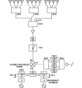 A 12-sector antenna smart base station provides increased coverage and capacity over the traditional three-sector system. Other SP4T products on the market require negative or positive/negative voltage supplies and up to eight control lines, and are housed in 24-lead wide body small outline ICs (SOIC) and 28-pin plastic leaded chip carrier packages. The smaller 14-lead SOIC size (0.080 sq. in.) incorporated in the SP4T version saves over 60 percent in PCB area vs. the more common (0.178 sq. in. to 0.240 sq. in.) packages.
The HMC183QS24 SP8T switch offers major benefits for adaptive switching functions in base stations, particularly savings in overall circuit size. The switch is the industry’s first monolithic SP8T available in a low cost SMT package with an integrated 3:8 decoder driver. The SP8T switch provides a single-chip solution, reducing an equivalent SP8T discrete layout area consisting of two SP4Ts and one SPDT by over 90 percent. For the larger multithrow configurations shown in the typical base station receiver, the four HMC192S14 SP4Ts could be replaced by two HMC183QS24 SP8Ts and one HMC190MS8 SPDT to select between the SP8Ts.  This configuration increases the available channels to 16, allowing for auxiliary or functional test inputs in parallel with the 12-element antenna receiver inputs. The 24-lead quality small outline package (QSOP) industry-standard plastic package occupies the same PCB area (0.080 sq. in.) as each HMC192S14 SP4T 14-lead SOIC. The HMC183QS24 SP8T switch is shown in Figure 2 .The HMC192S14 device, shown in Figure 3 , requires only +5 V of bias at < 5 mA and two positive-voltage CMOS-compatible control lines
  via an integrated 2:4 decoder. The RF1 to RF4 ports are nonreflective when in their off states. Figure 4 shows the SP4T’s insertion loss, return loss and isolation. With only 0.7 to 1 dB insertion loss per switch, the total front-end matrix path loss through two switches (plus PCB and mismatch losses) is 1.7 to 2.4 dB at the 900 and 1900 MHz cellular bands, respectively. Isolation between paths is defined by the 35 to 37 dB single-switch channel-to-channel isolation.
 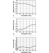 An input IP3 point of +43 dBm provides low distortion switching for technologies that demand a high dynamic range such as code-division multiple access (CDMA).
Another common BTS switch application is the selection of differential LOs in both the receive and transmit sections. This configuration can be accomplished using the new model HMC194MS8 high isolation SPDT switch. Less than 0.7 dB insertion loss is featured through 2.5 GHz. Isolation between channels is 50 and 42 dB at 1 and 2 GHz, respectively. Figure 5 shows the insertion loss and isolation for the ultra-small HMC194MS8 SPDT switch. 
Housed in an industry-standard eight-lead mini small outline package (MSOP) (50 percent smaller than an eight-lead SOIC and 40 percent smaller than an eight-lead shrink small outline package (SSOP)), the HMC194MS8, shown in Figure 6 , is controlled by positive CMOS-compatible control voltages.The MSOP package occupies an area of 0.118" ¥ 0.192" with a maximum height of 0.042" and a lead pitch of 25 mil.  Lead coplanarity is maintained to 3 mils. The RF1 and RF2 ports are reflective open circuits when in their off states.
The typical base station diagram shows the configuration of three HMC194MS8 switches into a high isolation terminated SPDT. One-quarter wavelength transmission lines are used between the common switch and each outrigger switch to enhance the doubled HMC194MS8 isolation by another 10 to 15 dB. This high isolation switching structure was designed and fabricated in house to demonstrate the performance of the HMC194MS8 switch in this base station application. Over 90 dB isolation at –40° to +85°C was achieved from 700 to 2000 MHz with only three model HMC194MS8 switches. Figure 7 shows the performance of this high isolation switch PCB assembly. Care was taken to decouple the six control lines and common Vdd bias lines running between the three switches. 
A High IP3 VVA for Cellular BTS
For level control of the incoming signal in the typical BTS receiver, the new positive bias/control 800 to 2000 MHz HMC173MS8 VVA is offered. Figure 8 shows the VVA’s input IP3 at –40°, +25° and +85°C, indicating it never falls below +20 dBm. Transmitter designers will find the HMC173MS8 VVA equally useful in the transmit power control loop just prior to the preamplifier.  Previous MMIC VVA designs offered poor power handling (0 dBm or less input 1 dB compression point (P1dB)) and poor linearity (+10 dBm or less IP3 at room temperature only).
Over 50 dB of attenuation range is available from 800 to 950 MHz and up to 30 dB range is obtained at 2000 MHz. The input P1dB is +16 dBm (typ) for any attenuation state and +10 dBm (min) over temperature, which is the best available power handling in the industry for GaAs MMIC VVAs. Housed in an industry-standard eight-lead MSOP package, the VVA is 50 percent smaller (0.022 sq. in.) than an eight-lead SOIC and 40 percent smaller than an eight-lead SSOP, which house other typical VVAs. Figure 9 shows the functional diagram of the HMC173MS8 VVA. 
Conclusion
Cellular BTS suppliers are working to meet the demands of cellular service providers and society in general to produce less obtrusive, aesthetically pleasing cellular sites and equipment. This new equipment must increase cellular coverage and subscriber capacity while improving overall communications quality. With these requirements in mind, cellular BTS engineers are demanding more performance, lower cost and smaller size from MMIC components. This new family of GaAs MMIC products can help BTS engineers meet their design objectives.
SPDT to SP8T monolithic switches with integrated drivers can help to improve and reduce the size of antenna, attenuator, filter and synthesizer matrices. The HMC173MS8 50 dB VVA with +21 dBm IP3 can help new systems meet their high dynamic range requirements. To augment these products, HMC175MS8 MMIC mixers in standard plastic packages offer high LO suppression, which is essential to reducing overall spurious levels in the RF/IF bands, and HMC187MS8 passive frequency doublers do not contribute phase noise while isolating the fundamental input by over 45 dB.
Hittite Microwave Corp. is an ISO 9001-registered company. For more information on these products, consult the company’s data book and Web site at http://www.hittite.com. S-parameters are available for seleted products and can be downloaded at the site. Samples are available for all products. Production quantities are available on tape and reel.
Hittite Microwave Corp. , Woburn, MA (617) 933-7267.