
SiGe MMICs and Flip-chip MICs for Low Cost Microwave Systems
Recent progress in SiGe device technology has improved cutoff frequencies of these devices to beyond 200 GHz. Such high speed transistors fabricated on low cost Si substrates allow high levels of integration as well as the development of low cost microwave circuits for consumer markets. As circuit speed increases to microwave and mm-wave frequencies, simple resistor-capacitor networks become inadequate and the need arises for distributed elements such as transmission lines. This article describes two approaches for implementing distributed structures with Si substrates: microstrip transmission lines using thick polyimide over a ground plane on the substrate (comparable to a conventional MMIC) and small Si devices or chips flip-chip mounted onto a microwave circuit board containing the distributed elements (comparable to a conventional MIC). Microwave circuits such as amplifiers, oscillators, mixers and frequency dividers have been demonstrated using both techniques.
Michael Case
Hughes Research Laboratories
Malibu, CA
In order to fully utilize the performance of high speed semiconductor devices, microwave components such as inductors, tuned matching networks, reactive loads and power splitters are required.1 MMICs using distributed elements such as transmission lines for such components are commonly implemented on semi-insulating (SI) III-V compound semiconductor substrates (GaAs or InP). Transistors and microwave circuits based on these substrates have demonstrated good results for more than 20 years.
Although GaAs- and InP-based MMICs have demonstrated strong performance at microwave and mm-wave frequencies, their cost remains too high for insertion into commercial applications. Typical foundry prices range from $1/mm2 for GaAs at low microwave frequencies (< 10 GHz) to $10/mm2 for InP mm-wave (> 40 GHz) circuits. These costs prohibit commercial use of all but the most simple MMIC or discrete device. The cost of typical high performance Si and SiGe bipolar technologies ranges from 10¢ to 40¢/mm2.
Recent improvements in Si1-xGex/Si heterojunction bipolar transistors (HBT) have increased cutoff frequencies to 50 to 200 GHz,2-4 approaching the cutoff frequencies of III-V HBTs and even high electron mobility transistors (HEMT). A significant problem with Si-based MMICs is the lack of a Si substrate. High resistivity silicon has been used,3 however, these substrates are often more costly than their III-V counterparts and are not always compatible with standard, industrial Si production lines. Two approaches are described for integrating distributed elements with high frequency Si devices: the polyimide microstrip MMIC and the flip-chip MIC. In the microstrip MMIC, shown in Figure 1 , the polyimide and gold that form transmission lines are deposited on top of conventionally processed Si wafers. For the flip-chip MIC, shown in Figure 2 , the flip-chip can be either a discrete transistor or a complex IC. The active die is attached to the passive substrate using solder bumps.
|
|
|
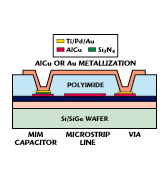
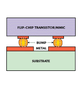
 Figure 3 shows a comparison between the losses of 50 W microstrip transmission lines using three different dielectrics with their typical thicknesses: 250 mm Duroid,6 100 mm GaAs and 13 mm polyimide.7 The polyimide loss is measured data; the Duroid and GaAs are calculations. Peaks in the measured data result from the measured line being an integer-multiple of a half-wavelength. (For example, the line's length L = nv/f, where n is an integer, v is the phase velocity on the line and f is the frequency.) For good dielectrics, the loss of a microstrip line is dominated by metal resistivity and, since a wider metal line is needed for thicker substrates to maintain the desired impedance, a thicker substrate generally will provide lower loss.
Polyimide Microstrip MMICs
Polyimide microstrip transmission lines consist of a metal ground plane, which is the top layer of metal on a standard processed Si IC wafer, and a thick layer of polyimide, which supports the microstrip line.5 This structure is then a conventional MMIC using the components from a standard Si IC process (transistors, resistors, capacitors and diodes) under the ground plane with the transmission line elements above. Such a structure makes highly integrated circuits possible, for example, by including microwave circuits (low noise amplifiers, mixers and oscillators) on the same chip as signal processing and digital circuitry.
Currently, work is being performed with 200 mm SiGe bipolar technology.2 In this variation of a standard Si IC process, three levels of metallization are used normally for interconnections. The top layer of metal is used as a ground plane for the microstrip transmission lines, but the ground plane must have openings to allow connections between the lines above and the devices below. The substrate, devices, interconnects and ground plane are all part of the standard IC process.
The first step in creating MMICs from standard ICs is the deposition of polyimide on top of the ground plane. Polyimide is a viscous liquid applied by squirting a small puddle in the wafer's center then spinning the wafer at high speed (1000 to 5000 rpm). The final thickness of the polyimide film, critical to the transmission line's impedance, depends on the viscosity of the liquid and the spin speed. After spinning, the wafer must be baked to cure the polyimide. Curing causes molecules suspended in the liquid to link together forming large polymer chains. The resulting material is a hard plastic-like coating on the wafer.
 The most important characteristic of the polyimide to affect microstrip performance is the amount of microwave energy that it absorbs. A common parameter to quantify this effect is the dielectric loss tangent tand, which is the ratio of the imaginary to the real component of the dielectric constant e(tand = e''/e'). Loss due to imperfect dielectrics is proportional to the product of frequency and the loss tangent. The polyimide used has a tand = 0.02.
After polyimide deposition, vias are etched to contact devices below using a reactive ion etch system. This system ionizes oxygen and freon to form a plasma that etches the cured polyimide. Figure 4 shows a scanning electron microscope (SEM) photograph of a typical via etched in 13 mm-thick polyimide.
The final procedure to complete the Si MMIC is deposition of the metal used for the transmission lines and other interconnections on top of the polyimide. Gold, which is used due to its low loss and corrosion resistance, is electroplated in the desired pattern. Aluminum could be used for compatibility with Si IC processes but is susceptible to corrosion.
The polyimide used to support the transmission lines is thick enough to allow relatively low loss microstrip, yet thin enough so that the vias are only 40 mm in diameter. Thicker polyimide would allow wider, hence lower loss lines, but would also cause the vias to be larger and present more parasitic capacitance. Since the polyimide cures at a low temperature (300¡C), there is no effect on the devices. The size of the final die may be larger than a typical IC since there are long transmission lines, but the polyimide MMIC process should be used only if necessary to obtain the desired performance.
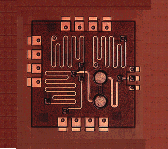
A variety of polyimide MMICs that combine the SiGe HBT devices2,3 with polyimide dielectric microstrip lines5 have been designed and tested. Figure 5 shows a Ku-band driver amplifier using polyimide transmission lines. The large circles are capacitors and the small circles are vias between devices under the ground plane and the microstrip lines. Figure 6 shows the amplifier's output power and gain vs. input power. The small-signal gain is 7 dB and the power output at 1 dB compression is 40 mW at 12 GHz.
|
|
|
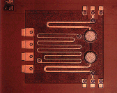
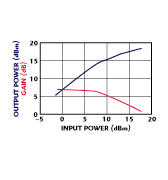
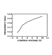
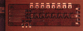
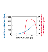
Figure 7 shows a Ku-band VCO with buffer amplifier. The distributed elements are implemented using polyimide transmission lines. The VCO's frequency vs. control voltage is shown in Figure 8 .A K-band static frequency divider (¸ 128) implemented with an inductively peaked input buffer at the left side is shown in Figure 9 ;8 its response is shown in Figure 10 . The divider's maximum operating frequency is 23 GHz. An X-band single-balanced mixer has also been reported.9
|
|
|
|
|
The polyimide MMIC allows high quality microstrip elements to be included in the design to enhance the circuit's performance and open the door to tuned elements, but there are drawbacks from traditional MMICs fabricated on SI substrates. Whenever a via is needed to access the devices below the ground plane, a large metal pad is required, which has a parasitic capacitance associated with it. This capacitance can be designed around, but can impose restrictions on the design. Furthermore, the polyimide itself can be sensitive to the physical environment. Temperature and humidity can affect the polyimide's loss and dielectric constant, which in turn change the transmission line's characteristics. Investigations are ongoing to determine how significant the parasitic capacitance and environmental sensitivity are and what limitations on the applications they may impose. 
Flip-chip MICs
Flip-chip IC attachment has been used widely in the IC industry recently to reduce the parasitics associated with the more typical wire bonding to packages. Flip-chip attachment requires a solder bump to be placed on the IC's pads. These solder bumps are then placed in contact with their desired pads on the package and heated to melt the solder, forming the connection.
The same flip-chip technique is used to attach small die (typically discrete transistors) to microwave circuit boards. Figure 11 shows a SEM photograph of a small die flip-chip mounted on a Duroid circuit board containing transmission lines and other distributed elements. The chip measures 1300 ´  1300 ´ 750 mm.Wire bonding, as shown in Figure 12 , has a large parasitic inductance that can change from bond to bond even in automated systems.
Typically, MICs contain a small number of discrete transistors and rely on transmission lines fabricated on a microwave circuit board for tuning to maximize their performance. The devices are typically wire bonded to the circuit board. The flip-chip MIC combines the repeatable, low parasitic attachment of solder bumps with the small die size and high performance achieved with an MIC.
In addition to repeatable, low parasitic connections, the flip-chip MIC approach allows a variety of technologies to be incorporated in a single circuit. For example, an InP-based HEMT chip can be used that has the lowest possible noise for an input amplifier, and a high speed SiGe analog-to-digital converter is placed on the same circuit. Many more combinations are possible, which can take advantage of the combination of technologies.
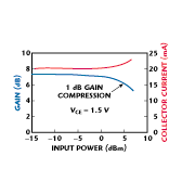
Several SiGe flip-chip MIC circuits have been designed and tested, combining SiGe HBTs with passive elements fabricated on 10 mil RO3010 Duroid. Small- and large-signal performances of a Ku-band amplifier are shown in Figures 13 and 14, respectively. This amplifier is similar to the Ku-band amplifier shown previously, but with a smaller device (40 mm2 compared to 100 mm2). The 1 dB gain compression occurs at 20 mW output power, approximately half of the output power from the Ku-band MMIC amplifier. Characteristics of a Ku-band frequency divider flipped onto a Duroid substrate are shown in Figure 15. Again, this divider is similar to the K-band static frequency divider shown previously, but the inductive peaking in the input buffer is eliminated and two additional divider stages are incorporated for a total division ratio of 512.
|
|
|
|

The flip-chip MIC offers an alternative to the polyimide MMIC. The approach to use is chosen depending on the system cost and die area consumed by the active components alone vs. a complete MMIC. Flip-chip attachment has proven its robustness in many IC processes. As long as the difference in thermal expansion between the Si chip and the substrate is considered (as well as temperature rise of the chip due to power consumption), a large temperature variation is not a problem. The most significant issue with the flip-chip MIC is accurate modeling of parasitics that arise from the lines on the chip between the devices and the bumps, as well as the bumps themselves. In this process, bump-to-bump spacing is approximately 100 mm. Electromagnetic simulations have shown substantial inductance and capacitance from feed lines even as short as these that impact tuned circuits as low as 10 GHz significantly.
Conclusion
Two approaches (polyimide MMIC and flip-chip MIC) have been demonstrated for implementing low loss distributed elements for integration with Si-based devices, and circuit results have been shown using both techniques. There is a trade-off that differentiates the two approaches. Although the loss of a transmission line on a thick Duroid board is much lower than that on thin polyimide, the parasitics associated with the lines on the Si-based die feeding the bumps and the bumps themselves impose difficult-to-model and often significant parasitics. The parasitics associated with the vias in the polyimide MMIC are much smaller. Furthermore, the lines on a thick Duroid board are much larger than on a thin polyimide, so overall circuit size is actually larger for the flip-chip MIC than for the polyimide MMIC; only the Si area is much smaller.
Solder bumps also have the potential to reduce the thermal resistance greatly between the junction of a device and its carrier since gold or silver bumps can be placed directly on top of active device areas. These solder bump characteristics, in conjunction with a thermally conductive substrate, make the flip-chip MIC attractive for high power microwave amplifier applications. The trade-offs of manufacturability, cost and performance must be explored to choose the proper technology.
Applications where these RF Si IC technologies would benefit due to the reduced cost and enhanced complexity are numerous. Highly functional microwave receivers could be made to enhance direct satellite communications to cover many different frequencies rather than the single-frequency units available currently. Electronically steered phased-array antennas may become household items if the cost of microwave phase shifters could be reduced, allowing mobile satellite communication or automated antenna pointing. In general, a low cost microwave technology would allow consumers to afford systems normally considered reserved for the military, such as radar and point-to-point microwave communications, and would enhance the performance and functionality of existing microwave systems.
Acknowledgment
Much of this work performed at Hughes Research Laboratories would not have been possible without Mehran Matloubian and Robinder Virk. The 200 mm SiGe bipolar technology is a product of IBM. n
References
1. G.D. Vendelin et al., Microwave Circuit Design, Wiley Interscience, 1990.
2. D.L. Harame et al., "A 200 mm SiGe HBT Technology for Wireless and Mixed-signal Applications," IEDM, 1994.
3. K. Strohm et al., "Si/SiGe MMICs," IEEE Transactions on MTT, Vol. 43, No. 4, April 1995.
4. L. Treitinger, "Silicon Technologies for Ultimate Speed ICs," IEEE Cornell Conference, 1995.
5. M. Case et al., "High Performance Microwave Elements for SiGe MMICs," IEEE Cornell Conference, August 1995.
6. RO3010, Rogers Corp., Chandler, AZ.
7. Cyclotene 3022, The Dow Chemical Co., Midland, MI.
8. M. Case et al., "A 23 GHz Static 1/128 Frequency Divider Implemented in a Manufacturable Si/SiGe HBT Process," IEEE BCTM Proceedings, October 1995.
9. M. Case et al., "An X-band Monolithic Active Mixer in SiGe HBT Technology," IEEE MTT-S, June 1996.
Michael Case attended the University of California at Santa Barbara from 1984 to 1993, earning his BS, MS and PhD degrees. His graduate work was completed under the guidance of Professor Mark Rodwell, studying nonlinear transmission lines for ultra-high speed pulse, impulse and harmonic frequency generation. Currently, Case is employed at Hughes Research Laboratories in Malibu, CA, where he is involved with emerging technologies, high speed and high power circuits, and novel power-combining techniques.