
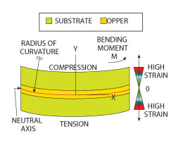
Figure 1 A PCB with a single conductive layer circuit with dielectric substrate material above and below, and the tension and compression that result from an applied bend radius.
Most RF/microwave printed-circuit-board (PCB) applications are planar and can be built with a flat circuit board. But some circuit applications may call for a PCB to be bent and formed into a three-dimensional (3D) shape. Bending PCB materials consistently and reliably can be challenging, and many circuit designers will confess to fractured conductors among other problems incurred during their initial experiences in trying to form a PCB into some nonplanar shape. Still, when the basic mechanical principles behind bending and forming PCB materials are better understood and properly applied, such as the capability to predict the minimum bend radius for a particular PCB construction, 3D circuits can be formed with reliable performance and without those fractured conductors.
A PCB consists of various materials, such as copper and dielectric layers. The layers are very different in terms of their mechanical properties and, accordingly, a PCB is considered a composite beam. When mechanical composite-beam theory is applied to the bending and forming of PCBs, there are four major areas of concern:
- The applied bend radius and related forces
- Strain on the different layers of the PCB
- The neutral axis location
- The modulus (stiffness of the different materials in the PCB).
A simple example may help to understand the basic concepts of bending a circuit. Although this example is not particularly common in the RF/microwave industry, it is well suited for describing the mechanical issues of bending a PCB. Once these issues are reviewed, some circuit configurations more commonly used in the microwave PCB industry will be considered. This simple initial example consists of a circuit formed on a single conductive layer of copper, with dielectric substrate on both sides of the copper. It is similar to the flexible printed-circuit construction used in very high dynamic flexing applications, such as the read-write servo arm interconnection inside a computer’s hard disk drive (HDD). Figure 1 shows a cross-sectional view of this simple single-sided circuit example, with an applied bend radius.
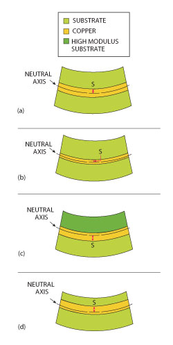
Figure 2 Neutral axis location and maximum strain(s) on one of the copper-substrate interfaces for balanced circuit (a), balanced circuit with thinner copper (b), geometrically balanced circuit with high modulus substrate on one layer (c), and offset balanced circuit with the same substrate material of different thicknesses (d).
If this circuit board was handheld and bent, the substrate would undergo compression on the inside of the bend and tension on the opposite side of the substrate. A transition from compression to tension would take place within the circuit material, occurring within an almost infinitely thin plane. Within this plane, called the neutral axis of the PCB, there is zero strain. For a balanced circuit board, the neutral axis is located at the geometric center of the board. The example circuit is considered a balanced circuit because it assumes that the substrate layers at the top and bottom of the copper layer have the same thickness and same modulus (stiffness). With thicker top and bottom substrate layers, more force is needed to achieve a given bend in the PCB. In such a case, even though the neutral axis will have zero strain, the amount of strain away from the neutral axis will be significantly increased compared to a circuit with thinner substrate layers.
Understanding the amount of strain at a specific material interface within a PCB is critical when trying to bend a circuit without fracturing its conductors. In general, the threat of fracturing copper is a concern for any copper-substrate interface that must endure strain of any kind. A crack that starts at this interface can propagate through the thickness of the copper, resulting in a fractured conductor.
A PCB’s neutral axis exhibits zero strain; the strain increases at any distance from the neutral axis. Essentially, further distance from the neutral axis translates into higher strain, and higher strain translates into increased potential for circuit fracturing. For the example circuit, a thinner copper layer will be a better choice for bending without fracturing the copper. For a PCB with thinner copper, the copper-substrate interface furthest from the neutral axis will be a shorter distance from the neutral axis than a PCB with thicker copper. For this reason, thin copper is used with the thin balanced circuitry inside HDDs.
Figure 2 shows the variations for this example circuit. In Figure 2a, the balanced circuit will have the same strain(s) on the top copper-substrate interface as on the bottom copper-substrate interface. This will also be true for Figure 2b, although with thinner copper, the copper-substrate interface will be closer to the neutral axis and will exhibit less strain. Figure 2c shows a geometrically balanced circuit (substrate layers of equal thickness). However, the top substrate layer uses high modulus substrate material, and the neutral axis will shift toward the high modulus material, creating a greater distance between the neutral axis and the bottom copper-substrate interface. With this high modulus substrate layer, this lower metal-substrate interface will suffer much more strain than the top copper-substrate interface. Finally, Figure 2d shows a circuit that uses the same substrate materials, although with a thinner substrate layer at the top than at the bottom. As a result, the neutral axis will shift toward the thicker material and create higher strain on the top copper-substrate interface.
The neutral axis location is a serious concern when bending and forming PCBs, but the modulus of the different layers within the PCB is also very important. The modulus has an impact on the neutral axis location as well as increasing the strain within the circuit. PCBs intended to be bent or formed should be fabricated with nonwoven glass reinforced materials. Many PCBs are constructed with woven-glass reinforcement. A woven-glass layer has areas of voids between knuckles of glass strands and these different areas of the woven-glass layer cause large transitions in modulus in isolated areas.Stress can be concentrated at these transitionsand high strains develop in these areas where the modulus value changes significantly over a short distance; such variations in modulus value can also be difficult to model. Due to these issues, circuit materials with woven-glass reinforcement should be avoided when fabricating a circuit that will be bent or formed.
The modulus values of the various materials used to produce a PCB can be significantly different. The modulus value for copper is typically the highest in a PCB, normally orders of magnitude higher than the modulus value of the substrate. Table 1 shows modulus values for various materials used in PCBs intended to be bent or formed.
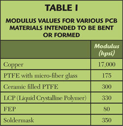

Figure 3 A microstrip transmission line circuit with an applied bend radius in three-dimensional view (a) and cross-sectional view with the isolated area of the signal conductor on top and ground plane on bottom (b).
Since copper is the highest-valued modulus component in a circuit construction, it is important to consider when evaluating mechanical models to reduce strain for better bending and forming capability. When considering the amount of strain within a circuit, reducing the amount of copper will reduce the overall strain. Copper can be reduced by making the various copper layers thinner, reducing the percentage of copper per copper layer, or reducing the number of copper layers.
To understand how bending and forming circuits can impact circuit designs employed in the microwave industry, it might be helpful to examine how bent circuits are made using microstrip transmission lines. Such circuits are often formed for 3D antennas and interconnections that are nonplanar. As an example, Figure 3 shows a simple microstrip transmission line with an applied bend radius. The neutral axis will be at different locations depending on where it is evaluated within the cross-sectional view of the circuit.
When bending and forming microstrip circuits, the signal layer is typically considered more critical than the ground plane for strain modeling and predicting copper fracturing. If micro-fractures appear on the ground plane copper, it will probably have less electrical impact than the narrower signal conductor. Following that reasoning, Figure 3b shows maximum radius Rmax as the high strain plane that would need to be modeled to predict copper fracturing during PCB bending and forming. In the case of the signal conductor, Rmax is at the furthest distance from the neutral axis.
To calculate values for the neutral axis and the percent strain, an Excel® worksheet can be created to predict those values. Predictions can be made based on the following equations for the neutral axis, R0, and the percent strain (% strain):
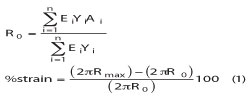
with Yi being the mean distance from the origin for each layer of material, where the origin is considered the bottom of the circuit where the bend radius is applied. Parameter Ei is the modulus of each layer within the circuit while Ai is the area of each layer. The neutral axis location, R0, is the distance from the origin or bottom of the circuit, as shown in Figure 3b.
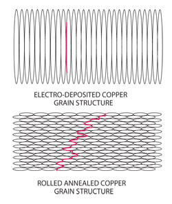
Figure 4 An exaggerated, simple comparison of standard ED copper and rolled copper. The red lines show potential for crack initiation and propagation for the different types of copper.
If performing calculations for different PCBs and different materials, it might be useful to have some strain values as guidelines or reference points. For example, studies have been done in the flexible circuit industry that give a correlation of strain to copper fracturing and when using smooth rolled copper the maximum strain is 2 percent. PCBs with rolled annealed copper handle bending and forming much better than PCBs with standard electrodeposited (ED) copper. Still, some confusion exists between these two copper types because of the way they are tested. PCB copper is typically tested for elongation within a plane, where a copper foil is pulled apart in a planar manner but without any bend. When a bend radius is applied, rolled copper will perform much better than standard ED copper due to its copper surface roughness and copper grain structure. Figure 4 offers an exaggerated and simple drawing to explain this issue. When a bend is applied to standard ED copper, the peaks of the surface will be pulled apart from each other and a crack will easily form. Once a crack is initiated in ED copper, the fracture will readily propagate through the thickness of the copper.
In the case of rolled copper and with an applied bend radius, there are no distinct stress concentrators and it is difficult for a crack to initiate. The smoother surface makes it more difficult for a crack to start and even if it does, the grain structure of the rolled copper does not allow the fracture to propagate easily through the thickness of the copper.
PCB bending and forming can be affected by copper and other plating materials applied to a circuit board. For example, a PCB with ED copper plated on top of smooth rolled copper can cause issues with bending and forming. Because copper is the highest modulus material in the PCB, the additional copper thickness is not desired and will raise the strain of the circuit board. Also, the plating of ED copper has a vertical grain structure that makes it easy for a crack to form when a bend radius is applied. The intermetallic boundary between the rolled copper and the ED copper plating can act as a stress concentrator and cause fracturing of the copper during bending and forming.
Electroless nickel/immersion gold (ENIG) plating is commonly used as a finish for PCB conductors. The same issues apply as mentioned with plating rolled copper with ED copper, however, an additional concern is that nickel is very brittle and can initiate fracturing easily when the circuit is bent.
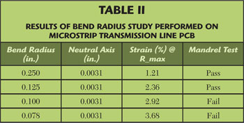
Bend radius is an important concern for PCBs that must be bent and formed. Put simply, a smaller bend radius will cause more strain on the PCB’s interfaces, resulting in conditions where fractures are more likely. To demonstrate the mechanical theory, a simple study was conducted where microstrip circuits of the same construction were bent around a controlled radius (metrology measurement mandrels). Many precautions were taken to ensure that the forces on the circuit were uniform around the mandrel when applying the bend radius. Table 2 shows the results of this study/model in terms of percent strain compared to the circuit bending information using different bend radius.
The mandrel testing results shown in Table 2 were produced using a simple microstrip transmission line circuit, made from a print/etch process and did not use plated throughholes (PTH). The PCB’s ½ oz. rolled copper did not have any copper plating on top, and no other finish or solder mask was applied (PCB used a 5 mil thick PTFE laminate). In addition, the pass/fail results from the mandrel test yielded a failed response when the circuit was found to have microcracks in the copper when inspected at 30×.
It should be noted that the value of 2 percent for maximum strain provided previously is a general guideline and that this value may appear to be conservative next to the results shown in Table 2. The 2 percent value is a general guideline and if a greater population of circuits was tested, a better trend might have been found for this particular example circuit construction.
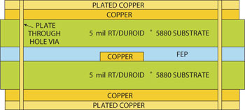
Figure 5 A cross-sectional view of a stripline transmission line circuit.
A real microwave application example, but a more difficult PCB construction to model is a stripline transmission-line circuit. The application requirements were that the circuit be bent once, bend radius of 0.200 in., circuit using 1 oz. copper and ENIG plating on the outer ground layers. The application required low insertion loss of 1.0 dB/in. or less at Ka-Band frequencies, specifically at 31 GHz.
Electrically, a thin laminate was needed, with low dissipation factor and smooth copper for minimal conductor loss. A PCB with lower dielectric constant would make it possible to use a wider conductor and reduce conductor loss. The material chosen was 5-mil-thick Rogers RT/duroid® 5880 laminate and is available in a minimum thickness of 5 mils with rolled copper. For the mechanical requirements, the laminate does not use woven-glass reinforcement and consists of low modulus substrate. Figure 5 shows a cross-sectional view of the stripline circuit used for this example.
For this example, it is possible to have relatively low strain on the internal signal layer, because the neutral axis will be very near this copper layer. However, the top and bottom ground planes will be very far from this PCB’s neutral axis and they will experience much higher amounts of strain when a bend radius is applied.
Several mechanical models were run and found changes had to be made. Table 3 shows the results of some of the mechanical models, using 1, ½ and ¼ oz. copper. As the values in Table 3 indicate, strain on the signal layer in the stripline example was not a concern. However, the higher strain numbers for the outer ground planes may be some cause for concern. The original model had strain figures of about 3.5 to 3.6 percent for the outer copper layers, a range where copper fracturing is a risk. After reviewing the specifications for the model, it became evident that the 1 oz. copper thickness could be reduced, making it possible to achieve improvements in strain values by using thinner copper layers in ½ and ¼ oz. copper circuit models.
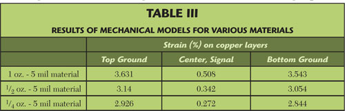
Even with thinner copper, strain values were 2.8 and 2.9 percent for the stripline models – of some concern, but accepted as being within the limits of the different tradeoffs for this study. To gain a real-world perspective, prototype circuits were fabricated based on the model parameters, then bent into shape and inspected for copper fracturing. These prototypes did suffer copper fracturing, so changes were necessary. After evaluating several different models and prototype builds, successful results were obtained by addressing a number of issues. For example, the original prototype circuits featured plated copper at an average thickness of 1.2 mils and this was reduced to an average of 0.5 mils. The thinner copper improved the strain numbers to about 2.2 percent.
The ENIG plating used in the first round of these stripline prototype circuits was also viewed as a potential cause of copper fracturing, and was replaced with immersion silver. Implementing these changes in the prototype stripline circuits improved their bending capabilities significantly, although a small percentage of problems existed when evaluating a large number of circuits after bending. It was then determined to heat the circuits during the bending process. The substrate is based on polytetrafluoroethylene (PTFE) and this material becomes softer (its modulus decreases) as it is heated. The same applies to the FEP bonding layer. Heating results in less strain during the circuit bending/forming process, improving upon the mechanical model. A heating fixture was assembled to form the circuit around a controlled mandrel and at a temperature of +250°F. After fine tuning the fixture to ensure even pressure was applied to the circuit, with strain evenly distributed, very good results were obtained.
There are always tradeoffs with any new circuit design. The same applies when considering mechanical engineering for a circuit. Understanding the multiple tradeoffs for the stripline circuit example is typical of the process required for obtaining a microwave PCB that can be bent and formed reliably.