
Design and Characterization of a Multipurpose PCS Class A Amplifier
E. James Crescenzi, Jr. and Walter A. Strifler
Watkins-Johnson Co.,
Microwave Products Group
Palo Alto, CA
The rapid expansion of personal communications service (PCS) base stations and services has resulted in an increased demand for linear power amplifiers in the 1.93 to 1.99 GHz band. Two of the most widely used PCS signal formats, code-division multiple access (CDMA) and North American Digital Cellular (NADC) time-division multiple access (TDMA), require that transmitter power amplifiers operate within strictly defined limits for signal distortion and spectral regrowth. Typically, single-channel base station PCS amplifiers produce 2 to 50 W of average output power. Multichannel amplifiers must be capable of yet higher levels to avoid interference resulting from the intermodulation of the several simultaneous signals. A wide variety of approaches have been taken to achieve high linearity at high powers. GaAs MMIC power amplifiers with class E and F modes of operation1 have demonstrated clear advantages for hand-held transceivers. Base station power amplifiers commonly use class A and A/B amplifiers and amplifier subsystems with predistortion,2 feedback3 and/or feedforward4 compensation. Even in high power designs with class A/B outputs, it is common to incorporate class A amplifier stages as drivers or as correction amplifiers in feedforward designs. The class A amplifier has become a multipurpose element of a wide variety of designs in which the amplifier may be operated well below its maximum output power capability. Therefore, it is essential to characterize the class A amplifier performance over a wide range of output powers and for a variety of signal types. The historic power at 1 dB gain compression (P1dB) and the output third-order two-tone intercept point (OIP3) are certainly of interest but are no longer sufficient characterization. PCS applications often require spectral regrowth measurements such as adjacent-channel power (ACP) and measurements of digital signal distortion such as error vector magnitude (EVM).
There is considerable current research activity in the area of modeling power amplifier performance in processing digital communications signals.5,6 Measurements over a range of output power levels are beginning to be published,7 but it remains an area where the practitioner may be frustrated by the lack of available data, particularly for the PCS band. This article discusses the design of a PCS class A amplifier with 2 to 10 W output capability (depending on the signal format and performance standard). The rationale for choice of devices in the preamplifier and output stages, and the general block diagram are presented. The amplifier characterization will be for output powers of +25 to +40 dBm (10 W), and will include gain compression, third-order two-tone intermodulation, spectral regrowth (ACP for CDMA and NADC pi/4 differential quadrature phase-shift keying (DQPSK) TDMA signals) and EVM for NADC pi/4 DQPSK TDMA signals. These data should be useful for planning base station subsystems as well as for comparison of competing designs and emerging technologies.
Amplifier Design
The initial amplifier design objective was to achieve a minimum of 2 W output for CDMA base station applications (QPSK, with a nominal 12 dB peak-to-average ratio), which led to a rough estimate that a nominal 10 W P1dB capability was needed. At least two commercial silicon bipolar power devices are now available for 2 GHz 5 W P1dB class A applications (silicon devices designed for class A/B operation are more plentiful), as well as several GaAs power FETs. After a survey of available devices, it was concluded that commercially available 5 W silicon bipolar devices were significantly less costly than their GaAs FET counterparts. There was some question as to whether GaAs devices were more linear than silicon bipolars, but it was decided to pursue the more economical approach until it might be demonstrated that a higher cost approach is necessary. When investigating available devices with outputs of 100 mW to 1 W, GaAs FETs were found to be cost competitive and, therefore, were chosen as the driver stages. It will be interesting to follow this competition between silicon bipolar and GaAs FET power devices in the future.
The block diagram of the amplifier is shown in Figure 1 . The input stages employ AH1 surface-mount GaAs FET ICs with a nominal +21 dBm power output at P1dB, which are notable for their unusually high linearity (OIP3 of +40 dBm) that is achieved simultaneously with a noise figure of 3 dB. It is helpful to have high IP3s for the preamplifier stages so that the overall amplifier cascade linearity will reflect the full capability of the output devices and not be compromised by preamplifier limitations. The preamplifier section consists of a single-ended AH1 followed by a temperature compensation attenuator and a balanced AH1 stage. The power stages of the amplifier consist of a single-ended bipolar stage driving an output balanced bipolar stage. The bipolar devices are model 1920A05 silicon bipolar transistors with a nominal +37 dBm power output at P1dB. The device's guaranteed performance is 11 dB minimum gain with 5 W output over 1930 to 1990 MHz (Vc = +26 V and Icq = 600 mA). This device is a packaged bipolar transistor with input matching elements contained in a metal-flanged ceramic package, as shown in Figure 2 .

Fig. 1: The mulistage PCS amplifier block diagram.
Fig. 2: Multistage amplifier devices.
The input stage contains microstrip matching elements at the input and output of the AH1 to minimize input SWR (typically 1.25) and maximize gain (typically 12 dB), whereas the matching circuitry of the balanced AH1 second stage is chosen to achieve gain flatness with somewhat reduced gain. Measured two-tone intermodulation and CDMA adjacent-channel power rejection (ACPR) for the input single-ended AH1 stage are shown in Figure 3 . Third-order intermodulation measurements (IM3) are for two tones separated by 30 kHz. The ACPR measurements are of the first adjacent channel (885 kHz offset). The CDMA signal is simulated with a model UFX-CDMA generator with a peak-to-average ratio of 12 dB. Note that the AH1 has an optimum region of operation for linearity. In this case, the block diagram was chosen such that the maximum power output of an individual AH1 is £ +12 dBm. At this level, the ACPR for a CDMA signal is at least 60 dB for 885 kHz offset for the preamplifier stages. This ACPR is low enough that the spectral regrowth of the complete amplifier chain will be dominated by the output device and thus will be the maximum available for that device (assuming its matching circuitry is nearly optimum).
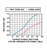
Fig. 3: AH1 IM3 and CDMA ACPR vs. output power.
The temperature compensation attenuator is programmed to provide temperature-dependent attenuation such that the overall amplifier gain is held constant over the operating temperature range of -45° to +70°C. The placement of the attenuator after the first stage (another alternative location would be after the second stage) optimizes power output and linearity at some expense in noise figure (typically 4.7 dB for the cascade). The output section of the amplifier is a single-ended bipolar stage followed by a balanced stage, all using the same 1920A05 devices. The output devices are biased at Vce = +25 V and Icq = 600 mA. Typical thermal resistance for these devices is 3.6°C/W. The estimated junction temperature is 131°C when the amplifier is mounted to a baseplate at +70°C. Figure 4 shows the complete model SA1056 multistage class A PCS amplifier. Typical characteristics are listed in Tables 1 and 2 .

Fig. 4: The SA1056 class A PCS amplifier.
|
Table I: Typical Digital Signal Characteristics | |||||
|
Digital Format
| |||||
|
Output Power (dBm) |
First Adjacent- |
ACPR (dB) |
| ||
|
CDMA QPSK (IS-95)* |
+33 |
750 |
-48 |
| |
|
CDMA QPSK (J-STD-019)* |
+33 |
885 |
-49 |
|
|
|
NADC TDMA pi/4 DQPSK |
+37 |
30 |
-32 |
|
|
|
*CDMA simulation with 12 dB crest factor noise spectrum in 1.23 Mhz band |
|
|
|
|
|
|
Table II: Typical Performance of a Multistage Class A PCS Amplifier | |
|
Frequency band (GHz) |
1.93 to 1.99 |
|
Gain at +25° C (dB) |
40 ±0.5 |
|
Gain vs. temperature |
±0.5 |
|
P1dB (dBm) |
+39 |
|
OIP3 (dBm) |
+4 |
|
Input/output SWR |
(1.3 |
|
Power supply (mA) |
1820 |
Multistage Amplifier Linearity Measurements
Measurement of amplifier performance when processing digital communications signals is a challenge to the RF/microwave designer. First, a familiarity with digital communications concepts9 and existing standards must be developed.10-12 It has also been determined that instrument suppliers and their applications staff are good sources of information. A model 2051 vector signal generator was chosen to produce the NADC (/4 DQPSK signal. This particular generator produces a 1.96 GHz NADC (/4 DQPSK signal with ACP of -38 dB (typ) and EVM of 0.7 percent (typ). The CDMA signal is simulated using a UFX-CDMA generator, which produces a band-limited spectrum of filtered and upconverted noise that has a peak-to-average ratio of 12 dB that is reportedly representative of a CDMA base station spectrum with one pilot, sync and paging channel, and six traffic channels.8 Signals from these sources are amplified by the device under test and then received using a model 89441A vector signal analyzer with the 89451A software option for digital communications signal measurements. The 89451A software is advantageous particularly for the analysis of NADC (/4 DQPSK signals in that it presets the instrument to assure compliance with IS-54 while making the relatively complex measurements. In particular, the vector signal analyzer incorporates root-raised-cosine filtering when making the ACP measurements and provides a pre-established set of channel definitions for these measurements. This area of standards interpretation is one of evolving consensus. Some controversy exists as to the proper method for making ACP measurements for NADC (/4 DQPSK signals. The ACP requirement of IS-54-B (page 72, paragraph 2.1.4.1.2) regarding limitations on emissions is stated tersely and the precise conditions associated with the measurement require interpretation (specifically the degree of overlap of the first adjacent 30 kHz channel with the primary channel).6 The data presented in this article for NADC TDMA signals assume no channel overlap. The impact of inclusion or exclusion of channel overlap is primarily a difference in the maximum theoretical ACPR (38.4 for no overlap and 35.8 dB with overlap), and it has a small effect at higher output levels (lower ACPR) typically required by amplifier specifications.13 In the CDMA case, there was no filtering internal to the analyzer and the power in 30 kHz adjacent channels was compared to the power in the main 1.23 MHz channel.
Typical measurements of the SA1056 amplifier are presented for a variety of tests. Figure 5 shows the normal two-tone output spectrum (+30 dBm per tone, 30 kHz spacing at 1.96 GHz) as observed with the vector signal analyzer. Note that the reference channel power and ACP measurements reference the power in two tones. For conventional notation (relative to a single tone), the first adjacent picket suppression of 40.9 dB implies an OIP3 of +49 dBm [(+33.0 - 3) + (40.9 - 3)/2)], approximately 1 dB less than is observed at low output levels (£ +23 dBm). Figure 6 shows the output spectrum for a 1960 MHz NADC (/4 DQPSK signal at the +37 dBm output level. The output power measured is that contained in the primary signal channel (as opposed to the total power including adjacent-channel spillover). The first and second adjacent channels are at 30 and 60 kHz offsets, respectively. The first adjacent channels of the measurements do not overlap with the primary channel. Figure 7 shows the constellation diagram and a summary of error vector measurements for the same signal conditions. IS-54 requires that the first ACP (±30 kHz) is below -26 dB, and that the second (alternate) channel (±60 kHz) ACP is -45 dB relative to the power in the main channel.

Fig. 5: The amplifier's output spectrum with two CW tones.
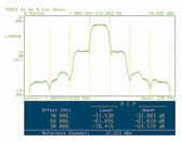
Fig. 6: The amplifier's output spectrum with a +37 dBm NADC (/4 DQPSK output.
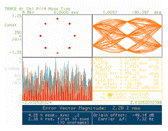
Fig. 7: The +37 dBm NADC (/4 DQPSK modulation output.
Typical measurements of the SA1056 amplifier with +34 dBm CDMA output power (in the primary channel) and a 12 dB peak-to-average ratio are shown in Figure 8 . In this case, the output is an unfiltered spectrum and the power in 30 kHz-wide channels at various offsets is compared to the power in the main 1.23 MHz channel. This definition, which incorporates different bandwidths for measuring the power automatically, produces an apparent 16.1 dB improvement (30 kHz/1.23 MHz) over what might seem like a reasonable interpretation of the output spectrum on a spectrum analyzer. The requirement for ACPR differs depending on the specification. IS-95 (the older, better-known specification for cellular systems) requires a minimum ACPR of -45 dBc at an offset of 750 kHz. The more recent standards proposal SP-3383 for PCS (scheduled to be issued as J-STD-019 in the near future) requires a minimum ACPR of -45 dBc at an offset of 885 kHz. IS-95 also requires an ACPR of -60 dBc at 1.98 MHz offset. The rejection for all three of these conditions is shown.

Fig. 8: The amplifier's output spectrum with +34 dBm average power for a CDMA input signal.
Characterization over An Extended Output Power Dynamic Range
The multistage amplifier was characterized for a wide range of output powers using the measurement techniques described previously. The two-tone intermodulation products of the complete chain show an approximate 3:1 dependence as a function of output power (2:1 for rejection), with a slight relative increase in level at higher output powers, as shown in Figure 9 . The output power for the two-tone measurement is the power per individual tone at 1.96 GHz with a 30 kHz spacing. A calculated OIP3 would range from +50 dBm (at +20 dBm output) to +37.5 dBm (at +35 dBm per tone - well into amplifier gain compression). Measurements of NADC TDMA signal characteristics for the amplifier are shown in Figure 10 over an average output power range of +25 to +40 dBm. ACPR for both 30 and 60 kHz offsets is presented. EVM is presented as total EVM and its components of magnitude and phase. Note that the ACPR is at least 35 dB for output levels below +35 dBm (EVM is < +30 dBm) are equal to those of the test equipment.

Fig. 9: The amplifier's two-tone IM3 suppression vs. output power.

Fig. 10: The amplifier's NADC TDMA ACPR and EVM vs.output power.
The results of testing with the filtered noise simulation of CDMA signals using the model UFX-CDMA generator with a 12 dB peak-to-average ratio are shown in Figure 11 for an output range of +27 to +38 dBm and for three offset frequencies (750, 885 and 1980 kHz). The measured first ACP level exhibits approximately 3:1 dependence (2:1 for rejection) on output power. Note that there is a good quantitative agreement between these measurements and the Wu model.14 The difference between the OIP3 and CDMA output level (to satisfy IS-95 specifications) is predicted to be 13.4 dB, which is close to the level observed in this work. Also, in this case, the CDMA backoff in output power below single-CW-tone P1dB is approximately 5 dB, significantly below published guidelines.
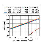
Fig. 11: The amplifier's CDMA ACPR vs. output power.
The normal minimum required ACPR (set by IS-95 and SP-3383) is -45 dB. Generally, in cases where this amplifier is embedded within a subsystem, it is desirable to operate in a region with significantly lower ACP. The ACPR data should be of value in planning CDMA subsystems incorporating linear amplifiers. It is important to note that differing class A designs (in topology, matching circuits and choice of devices) may exhibit significantly different ACP dependence on output power. Other classes of design, such as class A/B, can be expected to exhibit radically different ACP dependence on output power compared to the data in this article.7
Conclusion
A multistage PCS class A amplifier design has been presented, as well as the testing method for standard two-tone intermodulation and NADC TDMA and CDMA spread spectrum digital communications signals. This particular design applies GaAs surface-mount MMICs as preamplifiers and silicon bipolar power transistors in power stages. High dynamic range measurements of the amplifier were accomplished using specialized signal generators and a vector signal analyzer. The dependence of key amplifier performance characteristics such as ACPR and EVM was established over a relatively wide range of output power (+25 to +40 dBm).
Acknowledgment
The authors wish to acknowledge the technical assistance and contributions of John Bellantoni, Robert Buss, Eric Frick, Jay Kruse, Tom Spivey and Lisa To of Watkins-Johnson Co. The design of the power stages was facilitated by data and suggestions from Jerry Stambaugh of GHz Technology Inc., Santa Clara, CA. Helpful guidance in measurements as well as a constructive critique of the draft manuscript of this article were contributed by Robert Cutler and Ben Zarlingo of Hewlett-Packard Co. The AH1 GaAs FET IC is a product of Watkins-Johnson Co. The 1920A05 silicon bipolar transistor is a product of GHz Technology Inc. The model UFX-CDMA signal generator is from Noise/Com, Paramus, NJ; and the model 2051 vector signal generator is from Marconi Instruments Ltd., UK. The model 89441A vector signal analyzer and 89451A software are products of Hewlett-Packard, Santa Rosa, CA.
References
- Herbert L. Kraus et al., Solid-state Radio Engineering , John Wiley & Sons, 1980.
- S. Ogura et al., "A Linearized C-band Solid-state Power Amplifier for Satellite Use," 1994 Asia-Pacific Microwave Conference Digest , pp. 567-570.
- J.S. Cardinal and F.M. Ghannouchi, "A New Adaptive Double Envelope Feedback (ADEF) Linearizer for Mobile Radio Power Amplifiers," 1994 IEEE MTT-S International Microwave Symposium Digest , pp. 573-576.
- K. Konstantinou and D.K. Paul, "Analysis and Design of Broadband, High Efficiency Feedforward Amplifiers," 1996 IEEE/MTT-S International Microwave Symposium Digest , pp. 867-870.
- J.S. Kenney and A. Leke, "Power Amplifier Spectral Regrowth for Digital Cellular and PCS Applications," Microwave Journal , October 1995, pp. 74-92.
- J.F. Sevic and J. Staudinger, "Simulation of Adjacent-channel Power for Digital Wireless Communication Systems," Microwave Journal , October 1996, pp. 66-80.
- M. Shaw and A. Wood, "Characterization of a 2 GHz Submicron Bipolar 60 W Power Transistor with Single-tone, Multitone and CDMA Signals," 47th ARFTG Conference Digest, 1996 , San Francisco, CA.
- E. Garcia and B. Hessen-Schmidt, "Instrument Performs Multichannel CDMA Amplifier Testing," Microwaves & RF , May 1995, pp. 121-128.
- K. Feher, Wireless Digital Communications - Modulation and Spread Spectrum Applications , Prentice Hall Inc., 1995.
- EIA/TIA Interim Standard IS-54-B, "Cellular System Dual-mode Mobile Station/ Base Station Compatibility Standard," April 1992.
- EIA/TIA Interim Standard IS-95-A, "Mobile Station/Base Station Compatibility Standard for Dual-mode Wideband Spread Spectrum Cellular System," May 1995.
- TIA Standards Proposal SP-3383, "Recommended Minimum Performance Requirements for Base Stations Supporting 1.8 to 2 GHz Code Division Multiple Access (CDMA) Personal Stations." (If SP-8833 is approved, it will be published as J-STD-019).
- Clarification of the impact of the inclusion or exclusion of channel overlap was provided by Robert Cutler of Hewlett-Packard in a private communication.
- Qiang Wu, M. Testa and R. Larkin, "Linear Power Amplifier Design for CDMA Signals," 1996 IEEE MTT-S International Microwave Symposium Digest , pp. 851-854.