
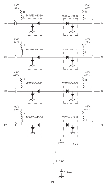
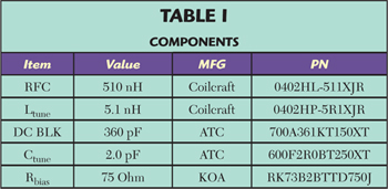
Figure 1 SP8T switch schematic.
Since their introduction more than 50 years ago, PIN diodes continue to be the technology of choice for the switching of medium to high power RF and microwave signals simultaneously with high linearity and fast switching speeds. Although transistor switches are able to perform switching functions with reasonably good RF performance, they often come up short compared to a PIN diode based design.
This article demonstrates the simplicity of designing what may be considered a complex single-pole-eight-throw (SP8T) switch using PIN diode SPICE models along with commercially available microwave CAD tools. Design principles highlighted include the use of EM simulations for developing an optimum center junction, the use of a nonlinear PIN diode model and a method for modeling the PIN diodes in a 2012 surface mount plastic package mounted on a substrate. The design is validated by comparing RF measurement to simulation. The results show that the PIN diode SPICE model provides a good fit to measured data and, therefore, minimizes the risk and potential additional costs associated with multiple design turns.
Design and Model
The application is a mobile transceiver that requires quick transitions between different RF channels along with good isolation. Size, cost and RF performance are all important considerations in the design of the switch that has the following goals:
- SP8T switch
- 1.2" × 1.2"
- 50 to 1000 MHz
- 1 dB insertion loss
- 30 dB isolation
- 15 dB IRL and ORL
- 20 W CW power
- 100 nSec RF switching speed with 500 nS pulse width and 10 percent duty cycle.
Figure 1 shows the circuit schematic. For this example, an Aeroflex / Metelics MSWSS-040-30 series-shunt PIN diode switch element (see Figure 2) is selected since it can handle the power and provides high linearity and high isolation in a small low cost 2012 surface mount package. The rest of the design uses a low cost FR-4 substrate, chip inductors and capacitors. The component values are given in Table 1.
The objective for the first part of the design is a center junction that presents an impedance as close as possible to 50 Ω at the input port with seven of the output ports turned off (capacitive loads) and only one of the output ports switched to a 50 Ω load. The structure, see Gardiol1, is modified for nine ports. When in operation, most of the ports look like capacitors (reverse biased series diodes). The port feeds are narrowed to make them look inductive; thus compensating for the capacitive loads. EM simulations were carried out while making iterative dimensional adjustments to the center junction to bring the input impedance as close as possible to 50 Ω (blue trace in Figure 3); then the input port was tuned with a series inductor and a shunt capacitor (green trace in Figure 3) to bring the input return loss (IRL) to more than 15 dB. The final center junction design is shown in Figure 4.
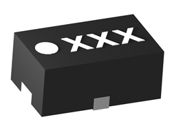
Figure 2 MSWSS-040-30 series-shunt PIN switch element with high isolation in a low cost 2012 surface mount plastic package.
An important factor in the center junction design is its dimension relative to a quarter wavelength (¼ λ). At 1 GHz, ¼ λ on FR-4 material (dielectric constant of 4.35) is equal to 1.4 inches, while the length across the final junction is only 0.295 inches (much less than a ¼ λ). If the frequencies were higher, and the wavelengths within the operating band were to approach the center junction dimension, then the center junction would need to be reduced in size to avoid transmission line effects that would make it more difficult to tune.
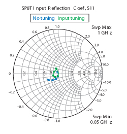
Figure 3 Center junction input impedance.

Figure 4 Final nine port center junction.
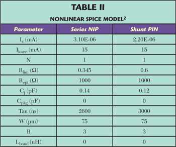
The second part of the design is the modeling of the PIN diode switch elements on the FR-4 printed circuit board substrate. The building blocks include the EM simulated center junction sub-circuit, the PIN Diode SPICE Models, the 2012 plastic package model, the Coilcraft inductor models and the ATC capacitor models. Table 2 provides the PIN diode parameter values and Figure 5 shows the 2012 package model with bond wires, transmission lines (for the package leads) and stray capacitance. The package leads are modeled as transmission lines sandwiched between two substrates — the plastic molding compound on top and the FR-4 below.
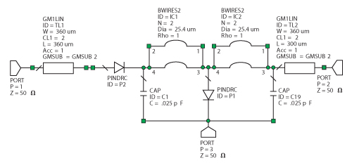
Figure 5 2012 package model with PIN diodes, bond wires, package leads and stray capacitance.
Representing one arm of the switch, Figure 6 shows the PIN diode switch element mounted on an FR-4 substrate with three vias to ground. To provide bias for the diodes, there is a discrete bias tee consisting of an RFC inductor, a DC blocking capacitor, a bypass capacitor and a bias resistor connected to a DC power supply.
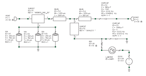
Figure 6 Package on PCB with RF choke, DC blocking capacitor, bypass capacitor, resistor and power supply.
The SP8T switch is less than 1 inch in diameter meeting the design goal of 1.2 × 1.2 inches; however, a final printed circuit board size of 2.37 × 2.58 inches (see Figure 7) is required to provide enough room for the bias terminals and RF SMA edge connectors.
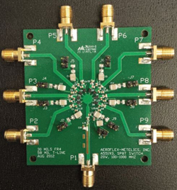
Figure 7 RF board actual size (2.37 × 2.58 inches).
RF Simulation Versus Measurement
The complete RF performance is summarized in Table 3. Overall, it is accurately predicted by the model. After subtracting out through losses, actual and modeled insertion loss agree to within 0.06 dB (see Figure 8). Isolation between non-adjacent channels agrees closely with the model at low frequencies and to within about 5 dB at the high frequency end. The deviation at higher frequencies is due to capacitive coupling. Isolation between adjacent channels — Port 1 to port 2 with port 3 turned on does not agree as closely. This is due to adjacent channel coupling not included in the model. Co-planar or ground metal between channels would improve this. The typical difference between simulated and measured results for this case is 15 dB (see Figure 8); however, the design still meets the 30 dB goal, because the series-shunt switch element provides a large amount of isolation.
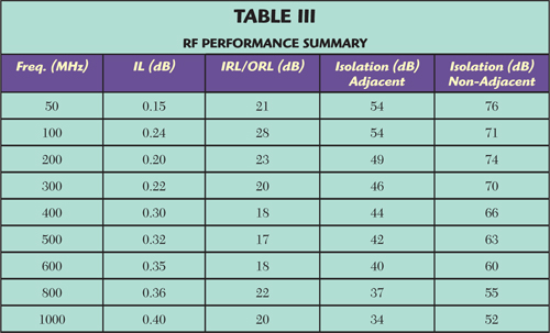
The modeled values of input and output return loss (see Figure 9), excluding the low frequency deviation due to the broadband capacitor used, are within 2.3 dB of measured. The worst case measured value of 17.1 dB is better than the 15 dB design goal.
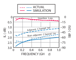
Figure 8 Insertion loss and isolation modeled (solid) vs. measured (dashed).
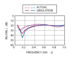
Figure 9 IRL and ORL modeled (solid) vs. measured (dashed).
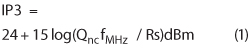
Often overlooked is one of the PIN diode’s biggest value propositions —linearity. In this case, the PIN diode’s 73 dBm third order intercept point (IP3) is higher than the measurement capability of the test system used. For this reason, the IP3 was calculated analytically using equation 1.2
Another advantage of PIN diodes, as compared to other types of switch elements, is the ability to switch large RF and microwave signals extremely fast. Using the Aeroflex / Metelics’ A55196 (rev -) driver circuit as an example, measured RF rise and fall times are 20 nSec and 15 nSec respectively, for a 500 nSec pulse width, 250 KHz repetition frequency and 20 W input power hot switched (see Figure 10). This is 44 times faster than the 450 nSec lifetime of the PIN diode and easily meets the 100 nSec design goal.
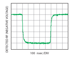
Figure 10 Detected RF switching speed with 20 ns rise time and 15 ns fall time.
Conclusion
A design methodology is presented which uses the PIN diode SPICE model and commercially available EM CAD tools for designing a SP8T switch. The model predicted IL to within 0.06 dB, IRL to within 2.3 dB and isolation between non-adjacent channels to within about 5 dB. Using a driver circuit, a switching speed of 20 nSec is achieved. The SPICE model combined with the EM simulation tool accurately predicts RF performance, minimizing the time and cost associated with multiple design turns. In this case, only a single design and fabrication turn was needed.
Acknowledgments
Thanks to Kam Lau, Rockford Curby, Francis Kwan, James Godbout, Rick Cory and Theresa Farris for their help in making this article possible.
References
- F.E. Gardiol, “Microstrip Circuits,” Wiley-Interscience, New York, NY, 1994, Section 6.7.2, pp. 119.
- R.H. Caverly and G.Hiller, “Distortion in P-I-N Diode Control Circuits,” IEEE Transactions on Microwave Theory and Techniques, Vol. 35, No. 5, May 1987, pp. 492-501.