
Editor’s note from Harlan Howe Jr.:
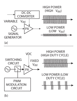
Figure 1 Transmitter block diagrams based on: bias modulation (a), PWM (b).
Pulse width modulation (PWM) has been the preferred method for control of electric automobiles as well as speed control for robot motion, because of its very high efficiency. However this is the first time that I have seen it applied to a power amplifier. The authors have presented a design that provides improved PAE efficiency at peak power and almost double the PAE at the 6 dB back-off point compared to previous works. While this amplifier is an RF design, there is no reason why PWM could not be applied to a microwave power amplifier.
This article describes a high efficiency Class E transmitter that produces variable output power using pulse width modulation (PWM) to maintain high efficiency. The system consists of a Class E power amplifier and a PWM generator. To reduce matching losses, high-Q inductors are used in the resonator. Low second and third harmonic distortion is achieved with a harmonic filter in the output matching network. It exhibits high power added efficiency (PAE) of 90.5 percent at an output power of 10.1 W. PAE at a low output power of 1.5 W is greater than 80 percent. The second and third harmonic distortion levels are as low as –35.1 and –44.0 dBc, respectively, at an output power of 10.1 W.
For efficient RF power transmission, transmitters need to have high efficiency. For power amplifier components, this reduces maintenance costs and cooling system requirements. Extensive research has been carried out using switching mode power amplifiers (SMPA) to improve power amplifier efficiency.1-7 Class D and Class E amplifiers are representative SMPAs. The Class E power amplifier considered here has a simpler circuit design and a higher operational frequency range than its Class D counterparts.8-10
For many applications, and especially for adaptive wireless power transmission systems, power transmitters are required to have variable output power to maintain high efficiency over a wide output power range. Typical power amplifiers, however, have a significant efficiency drop as the output power level becomes lower. In order to overcome this limitation, a bias modulation technique can be employed.11-13 This requires a DC-DC converter that has a variable output voltage. The output of the DC-DC converter is applied to the power amplifier as a drain bias, making the system more complex and expensive.
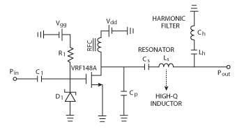
Figure 2 Schematic diagram of the 10 W Class E power amplifier with harmonic filter.
In this article, we propose a high efficiency power transmitter that has variable output power. It is based on a Class E power amplifier using a pulse width modulation (PWM) technique. It also includes harmonic filtering. As the duty cycle of the PWM signal decreases, the average output power of the transmitter is also reduced while theoretically maintaining efficiency as high as its peak value. By avoiding the need for a DC-DC converter, the circuit becomes significantly simpler. To verify this technique, a Class E transmitter with an output power of 10 W at 13.56 MHz was built and tested.
Principle of Operation and Circuit Design
Figure 1 shows block diagrams of the conventional and proposed transmitters. The conventional transmitter employs an adjustable DC-DC converter to provide the power amplifier with variable bias to change its output power level. Figure 1a shows that the peak output signal level is reduced as the drain bias voltage is decreased. The DC-DC converter should have high efficiency throughout its range, but the amplifier may not.
Figure 1b shows a PWM generator providing a pulse-width modulated sinusoidal signal at the input to the power amplifier driving it from zero to its peak output amplitude. As the duration of the PWM output is decreased, the average output power level of the amplifier decreases as well. Hence, the power amplifier has either a peak or zero-amplitude output signal. The amplifier is always driven to a region in which it operates most efficiently.
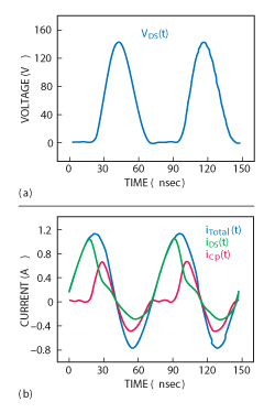
Figure 3 Simulated voltage and current waveforms: drain voltage and current (a), current to the shunt capacitor and total current (b).
A schematic diagram of the Class E power amplifier with a harmonic filter is shown in Figure 2. The output network of the amplifier consists of a shunt capacitor (Cp), a series resonator using capacitors and inductors for proper Class E operation and a shunt harmonic filter to remove the second and third harmonics. The inductance and the harmonic filter also provide fundamental matching. A Zener diode, D1, protects the circuit by clipping excessive input voltage to the transistor.
An ideal Class E power amplifier can achieve an efficiency of 100 percent based on its zero voltage switching (ZVS) characteristics. This means non-zero voltage and current waveforms of the transistor are shaped to not overlap each other. Non-ideal switching operation and insertion loss of the output network for practical Class E power amplifiers, however, cause efficiency degradation. The Q-factor of the resonator’s series inductor has the largest impact.14 We used a custom designed high-Q inductor to make the output power loss, i.e., efficiency degradation, as low as possible.
Agilent’s Advanced Design System (ADS) was used to design the Class E power amplifier. Figure 3 shows the simulated drain voltage and current waveforms for a drain bias voltage of 50 V and an output power of 40 dBm. A peak voltage of 142 V is approximately 2.8 times larger than the drain bias voltage. Due to the internal parasitic capacitance, the waveforms exhibit some non-zero overlapping. Each component in the output network has been fully optimized to have high efficiency, so we are confident that non-zero overlapping at the internal current source of the transistor is minimized. The simulation results yield a power gain of 23.6 dB and a high power-added efficiency (PAE) of 93.7 percent at an output power of 40 dBm using a 13.56 MHz continuous wave (CW) signal.
To change the average output power, the RF signal is repeatedly turned on and off using the variable PWM generator to adjust the duty cycle. Figure 4 shows a schematic diagram of the PWM generator. It consists of a three-stage OP amp which generates a 165.57 Hz pulse signal whose duty cycle can be adjusted using a tuning voltage (Vr). The 165.57 Hz pulse signal and 13.56 MHz oscillator output signal are fed to the NAND gate to form the PWM signal. Figure 5 shows the simulated output waveforms of the pulse generator with duty cycles of 0.9 and 0.1. By changing Vr, the duty cycle can be changed from 1 to 0.
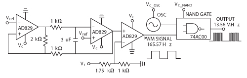
Figure 4 Schematic diagram of the PWM generator.
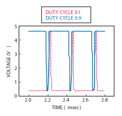
Figure 5 Simulated signals of the pulse generator.
Implementation and Experimental Results
A photograph of the 10 W Class E transmitter using the PWM technique is shown in Figure 6. Using FR4 substrate, which has a relative permittivity of 4.6, the circuit is approximately 115 × 36 mm2. Microsemi’s VDMOS FET, VRF148A, which has a breakdown voltage of 170 V, is used as the active transmitter device. To reduce matching losses, high-Q passive components are used in the matching network. The measured inductance and Q-factor of the custom-made series inductor at the output matching network are 1.3 and 300 uH, respectively. The NAND gate is a Fairchild 74AC00. An EXA XC300H13563TEH is used for the 13.56 MHz crystal oscillator. The PWM generator uses Analog Device’s AD829. Figure 7 shows the measured output waveforms of the PWM generator at various duty cycles. The duty cycle can be adjusted from 0 to 1 using Vr, which ranges from 5.5 to 3 V.
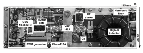
Figure 6 Photograph of the implemented 10 W Class E power transmitter based on the PWM method.
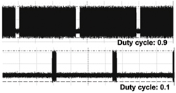
Figure 7 Measured output waveforms of the PWM generator at various duty cycles.
Figure 8a shows the measured PAE for three conditions: (1) input power control, (2) drain bias control using the conventional bias modulation method with a fixed input power, and (3) duty cycle control for the proposed PWM method with a fixed input power. When the input power is used to change the output power from approximately 10 W to almost 0, the efficiency drastically decreases. PAE based on the PWM technique, however, has a very similar trend as the conventional drain bias control method even without considering losses due to the conversion efficiency of the DC-DC converter. At a low output power of 1.5 W, the efficiency using the PWM technique is roughly 80 percent.
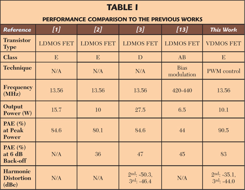
Figure 8b shows simulated and measured harmonic distortion levels of the Class E transmitter as a function of output power level. Both second and third harmonic distortion levels are lower than –34 dBc for all output power levels due to the harmonic filter in the output matching network. Second and third harmonic distortion levels are –34 and –43.6 dBc, respectively, at an output power of 10.1 W. Table 1 compares the results obtained from this work with those from other published works, showing significant improvement in efficiency at peak and 6 dB backed-off power levels.
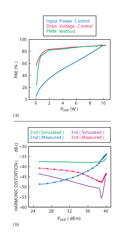
Figure 8 Measured performance of the Class E power transmitter: efficiency (a), second and third harmonic distortion (b).
Conclusion
In this article, we propose a high efficiency Class E variable output power transmitter using a PWM technique. The PWM generator in the transmitter modulates the input signal of the amplifier with pulses of various duty cycles, allowing the power amplifier to have high efficiency at a low average output power level. This method is simpler than that of a transmitter based on the conventional bias modulation technique, which requires a DC-DC converter having a variable output voltage.
The Class E power amplifier in this work employs a harmonic filter in its output matching network. The high-Q inductor in the series resonance circuit and the shunt harmonic filter also provide matching at the fundamental frequency. The second and third harmonic distortion levels are significantly suppressed. Based on the proposed PWM and harmonic filtering methods, a 10 W power transmitter was designed and implemented for the 13.56 MHz band. It exhibited a high PAE of 90.5 percent at an output power of 10.1 W and 80 percent at a low output power of 1.5 W.
Acknowledgment
This work was supported by Future IT Research Center, Samsung Advanced Institute of Technology.
References
- P.M. Gaudo, C. Bernal, and A. Mediano, “Output Power Capability of Class E Amplifiers With Nonlinear Shunt Capacitance,” IEEE MTT-S International Microwave Symposium Digest, Vol. 2, June 2004, pp. 891-894.
- J. Choi and C. Seo, “Wireless Energy Transmission High-Efficiency DCAC Converter Using High-Gain High-Efficiency Two-Stage Class E Power Amplifier,” Journal of Electromagnetic Engineering and Science, Vol. 11, No. 3, September 2011, pp. 161-165.
- M. Seo, J. Jeon, I. Jung and Y. Yang, “A 13.56 MHz High-Efficiency Current Mode Class D Amplifier Using a Transmission-Line Transformer and Filter,” Asia-Pacific Microwave Conference Proceedings, December 2011, pp. 1262-1265.
- M.W. Saito, T. Domon, I. Omura, M. Kuraguchi, Y. Takada, K. Tsuda and M. Yamaguchi, “Demonstration of 13.56 MHz Class E Amplifier Using a High-Voltage GaN Power-HEMT,” IEEE Electron Device Letters, Vol. 27, No. 5, May 2006, pp. 326-328.
- F.H. Raab, “Class E, Class C, and Class F Power Amplifiers Based Upon a Finite Number of Harmonics,” IEEE Transactions on Microwave Theory and Techniques, Vol. 49, Issue 8, August 2001, pp. 1462-1468.
- T. Mury and V.F. Fusco, “Inverse Class E Amplifier With Transmission-Line Harmonic Suppression,” IEEE Transactions on Circuits and Systems I, Regular Papers, Vol. 54, No. 7, July 2007, pp. 1555-1561.
- T. Suetsugu and M.K. Kazimierczuk, “Design Procedure of Class E Amplifier for Off-Nominal Operation at 50 Percent Duty Ratio,” IEEE Transactions on Circuits and Systems I, Regular Papers, Vol. 53, No. 7, July 2006, pp. 1468-1476.
- N.O. Sokal and A.D. Sokal, “Class E - A New Class of High Efficiency Tuned Single-Ended Switching Power Amplifiers,” IEEE Journal of Solid-State Circuits, Vol. 10, Issue 3, June 1975, pp. 168-176.
- N.O. Sokal, “Class E High-Efficiency Power Amplifiers, From HF to Microwave,” IEEE MTT-S International Microwave Symposium Digest, June 1998, pp. 1109-1112.
- J.F. Davis, and D.B. Rutledge, “A Low-Cost Class E Power Amplifier With Sine-Wave Drive,” IEEE MTT-S International Microwave Symposium Digest, Vol. 2, June 1998, pp. 1113-1116.
- F.H. Raab, “Intermodulation Distortion in Kahn-Technique Transmitters,” IEEE Transactions on Microwave Theory and Techniques, Vol. 44, Issue 12, December 1996, pp. 2273-2278.
- P. Draxler, S. Lanfranco, D. Kimball, C. Hisa, J. Jeong, J. Van de Sluis and P.M. Asbeck, “High Efficiency Envelope Tracking LDMOS Power Amplifier for W-CDMA,” IEEE MTT-S International Microwave Symposium Digest, June 2006, pp. 1534-1537.
- K. Narendra, A. Mediano, C. Paoloni and E. Limiti, “A Novel Adaptive LDMOS Power Amplifier with Constant Efficiency for Wide Dynamic Power Levels Control,” IEEE MTT-S International Microwave Symposium Digest, June 2008, pp. 1493-1496.
- N. Khalid, J. Singh, H.P. Le, J. Devlin and Z. Sauli, “A Very High Q-factor Inductor Using MEMS Technology,” Asia Pacific Conference on Postgraduate Research in IEEE Microelectronics & Electronics, January 2009, pp. 77-80.