
A Multilayer Microstrip Patch Antenna Subarray Design Using CAD
This article describes the design and development of an X-band, linearly polarized 4 × 4 element aperture-coupled microstrip patch antenna (ACMPA) subarray with a corporate feeding network. To reduce the design cycle time, commercially available CAD software packages are utilized in the antenna design process. The Ensemble® software package is used to obtain dimensions of a single multilayer microstrip patch antenna element. The feed network for the subarray is optimized using Touchstone® software. The overall design is verified experimentally by performing return loss, radiation pattern and gain measurements. This experimental part is useful in determining the accuracy of the CAD tools and in making small dimensional adjustments so that the final design meets the required specifications.
Hyok-Jae Song and Marek E. Bialkowski
The University of Queensland
Brisbane, Queensland, Australia
Small planar arrays incorporating microstrip patch elements are useful as building blocks in radar transmit/receive modules, direct-broadcast service television receive antennas, automatic road pricing systems and local multipoint distribution service. For many years, edge-fed microstrip patch antenna elements have been used to build such small subarrays because these elements offer an attractive planar format, low profile and low manufacturing cost. One disadvantage of these elements is that they offer a small operational bandwidth in the range of one to five percent. Because of their small operational bandwidth, edge-fed patch elements are found unsuitable in newly emerging wireless multimedia applications (for example, interactive television), which require an operational bandwidth in the range of 10 percent.
To increase the operational bandwidth of the microstrip patch antenna, different bandwidth enhancement techniques can be applied.1 One technique is to increase the thickness of the radiating patch substrate layer. However, this method cannot be applied easily to the edge-fed patch, a maneuver that would result in a considerable increase in the width of the feeding line, which would adversely affect the radiation pattern of the antenna. A feasible solution is to use an aperture-coupled microstrip patch in which the patch substrate layer can be modified without affecting the feed layer. In this arrangement, a thick substrate can be used for the patch layer and a thin substrate can be applied for the feed layer. However, the solution involving thick substrates may be unattractive for two reasons. The thick commercial substrates are significantly more expensive than their thin counterparts and, therefore, their use may lead to a substantial increase in the cost of the subarray. In addition, the thick dielectric substrate supports a surface wave that results in radiation losses.2,3 Also, diffraction effects (for the finite-size substrate) become more pronounced and lead to antenna radiation pattern perturbation.2,3 To eliminate these drawbacks, an ACMPA that uses lightweight and inexpensive plastic foam material to enhance the operational bandwidth is chosen. The plastic foam is inserted between the patch and feed layers to increase the patch layer height and, consequently, the operational bandwidth of the antenna. This arrangement provides structural rigidity and minimizes the effects of air gaps. This configuration choice is similar to one presented previously.4 However, the design approach is different.
Having chosen a suitable microstrip patch antenna configuration for bandwidth enhancement, this article concentrates on the use of commercial software packages to design and develop an X-band, linearly polarized, 4 × 4 element subarray. Design steps using suitable combinations of software packages available commercially are described.
CAD Tool Use
In the past, the design of a microstrip antenna was based mainly on the cut-and-try approach due to the unavailability of suitable CAD software. This approach has been problematic, particularly at microwave and mm-wave frequencies because of the extremely sensitive behavior of a patch radiator to small dimensional changes. This situation is improving slowly with the development of new antenna design software by a number of researchers. Although often limited in use, this new software has led to a more predictive way of designing edge-fed, proximity-coupled and aperture-coupled patch antenna elements and arrays.2,4-7
In the commercial market, only a few new CAD software packages can handle multilayer printed antennas simultaneously, including edge-fed, proximity-coupled and aperture-coupled elements. One of these software packages is Ensemble. This CAD package not only helps to design an ACMPA element, it also aids in the array's circuit layout production.9,10
Using Ensemble, an antenna structure must be meshed before the analysis can commence. Mesh size can be optimized using the auto meshing tool, which is included in the package. A finer mesh size must be chosen to obtain a more accurate analysis. However, simulation of more than a few elements with finer mesh size using Ensemble requires a considerable amount of computational time. For example, for the investigated 2 × 2 element X-band subarray with 1859 meshing cells and 11 frequency points, the required computer time on a Pentium 133 MHz PC was one hour and 17 minutes. The same subarray with 723 meshing cells, which was created by the auto meshing tool for a lesser accuracy, took only 14 minutes. Comparisons between the measured and simulated (for different mesh sizes) return loss plots for the 2 × 2 element subarray are shown in Figure 1 . 
Fig. 1: CAD analysis simulation with different mesh sizes.
From these comparisons, it is evident that Ensemble is a useful CAD tool for the design of a single ACMPA element and small subarray (2 × 2 element). However, to design a larger 4 × 4 element multilayer antenna subarray, Ensemble may face some memory and computational time difficulties. Therefore, a new design strategy is required that relies on the combination of three software packages: Ensemble, Touchstone and PCAAD (plus the experimental verification).
Using this approach, Ensemble is used to obtain the dimensions of a single ACMPA. The same package is also used to study the effects of mutual coupling for two elements as they would appear in the subarray. This procedure allows for the adjustment of antenna element dimensions for the assumed frequency band. Having obtained the single antenna dimensions that account for the mutual coupling effects, a corporate feed network is designed. It is assumed that antenna elements can be represented by lumped impedances, and Touchstone software is used to simulate and optimize the microstrip feed network under such conditions. To predict the radiation pattern and gain of the 4 × 4 subarray, the PCAAD software package is used. A summary of available CAD packages used in the design of an ACMPA and subarray is listed in Table 1 .
|
Table I: Commercially Available Microstrip Antenna/Circuit CAD Packages | ||
|
CAD Package |
Theoretical Model |
Design Application |
|
Ensemble |
full-wave/moment method |
patch antenna element design |
|
EEsof Touchstone |
- |
feed network synthesis/optimization |
|
PCAAD |
cavity model |
radiation pattern and gain prediction |
The Design
The objective is to design and develop an X-band, linearly polarized 4 × 4 element subarray that would feature approximately 10 percent operational (impedance) bandwidth with a flat gain performance centered at 10 GHz. Aperture-coupled elements employing thin substrates and inexpensive foam material for bandwidth enhancement are used. The design is divided into three distinctive stages: the antenna element design, the array optimum size and element spacing, and the subarray feed network design.
The Aperture-coupled Patch Antenna Element
The antenna element configuration chosen is shown in Figure 2 . This antenna element is formed by two dielectric substrate layers and two foam layers. RT/Duroid® 5880 with a dielectric constant of 2.2 and thickness of 1.57 mm is used for the patch layer. This material is followed by an inexpensive plastic foam to enhance the antenna operational bandwidth. An Ultralam® 2000 substrate of 0.762 mm thickness with a dielectric constant of 2.5 is used for the feed layer. This layer is followed by a foam layer with a thin copper deposited film to minimize the backward radiation. As such, this layer can be considered optional. Its thickness is close to a quarter of the waveguide wavelength to create a virtual open circuit at the aperture/feedline plane. The relative dielectric constant of the foam material, as measured using the HP85070B dielectric probe kit, was found to be within the range of 1.03 and 1.09 over the frequency band of 10 ±0.5 GHz.
 Fig. 2: The ACMP antenna element's (a) layout and (b) cross section.
The ACMPA element is designed for a given load impedance ZL, which in the present case is 50 ohm. The Ensemble CAD tool is applied to obtain the initial dimensions of the rectangular patch and slot for operation at 10 GHz. The parameters, which then are varied, include width and length of the patch, width and length of the aperture, and length of the microstrip stub. The thickness of the first foam layer also can be made variable. However, in practice, the variation of this parameter is restricted to a few discrete values. The remaining dimensions remain fixed. The antenna configuration is input easily using built-in drawing routines in Ensemble. The meshing required in the analysis is obtained automatically. The user must only provide the information about the mesh size. A finer mesh is usually required for a more accurate analysis. A few manual iterations are required to obtain satisfactory dimensions of the structure for an assumed return loss performance. Each of these iterations requires small dimensional adjustments, which are made easily using built-in procedures for shrinking or extending the antenna's dimensions.
Using satisfactory results for the return loss, the antenna element can be manufactured using standard photolithographic techniques. In this case, the antenna multilayer layout can be obtained directly using Ensemble by making layout transitions from BGF (Ensemble) format to DXF (AutoCAD®) format, which can be translated further to a more popular format such as HPGL or GERBER. An alternative approach is to use Touchstone with layout capability. In this case, the antenna element configuration must be redrawn, a simple and straightforward task that can be accomplished in a short time. The substrate layers then can be developed through chemical etching and the antenna element can be assembled.
Having developed a single antenna element, tests in terms of input return loss are performed using a vector network analyzer. In this case, the results for the return loss (S11 ) as obtained from Ensemble are compared with the measured values. From this comparison, the deviation between the CAD tool's analysis and the measured values is identified. The usual discrepancy concerns the frequency of operation and appears as a frequency shift in the return loss plot. The detected deviation (in the range of two to three percent) is taken into account in the next iterations in which the antenna's dimensions are adjusted so that the required return loss performance over a given frequency band is achieved. In the subarray design presented, the patch antenna was designed at 9.9 GHz instead of 10 GHz so that the 4 × 4 subarray could resonate at 10 GHz as planned. Using this approach, a single iteration step is needed to achieve the desired performance of an ACMPA with an impedance bandwidth (defined as a frequency range for which SWR
The same Ensemble package also can be used to study mutual coupling effects in the subarray. For this purpose, the analysis of E- and H-plane two-element arrays can be performed. For a given interelement spacing (as it is chosen in the planned subarray), the input impedance can be calculated. As the E-plane arrangement exhibits stronger influence on the input impedance, the dimensions of the patches can be adjusted for this case so the return loss performance is corrected and behaves as specified. (From the feedline point of view, the antenna's input impedance is approximately 50 W over a specified frequency band.) In the present case of the 4 × 4 element subarray, this adjustment was unnecessary since the frequency shift in return loss for the E-plane was one percent.
Feed Network Design
The corporate feed network is designed assuming that the antenna elements can be represented as lumped resistors (50 ohms, in the present case). This approach has been used already.8 The element spacing is chosen to be 0.8 wavelengths which offers a good compromise between the side lobe levels (SLL) and the antenna gain.
Figure 3 shows a general structure of the basic corporate-fed 2 × 2 element subarray for operation with a 50 ohms transmission line, which is later extended to the 4 × 4 element size. The feed network splits an original signal into four signals of equal magnitude and phase that, in turn, are fed to individual antenna elements. The feed network incorporated quarter-wave transformers, which provide impedance transformations between the load impedance and other characteristic impedances of transmission lines in the network.
 Fig. 3: The 2 × 2 element building block.
The role of the Touchstone software package is to optimize the input return loss of the feeding network, including discontinuities associated with impedance steps and T-junctions. This process is automatic provided the user inputs the configuration and substrate parameters of the microstrip feeding network. Once satisfactory results for the return loss have been obtained, the feeding network can be laid out and developed automatically.
Antenna Testing Results
Using the design steps described previously, a 4 × 4 element subarray was designed and manufactured for operation at 10 GHz. The manufactured 4 × 4 element subarray is shown in Figure 4 . Figure 5 shows the return loss plots of a single ACMPA element and a 4 × 4 element subarray as measured with a vector network analyzer.
 Fig. 4: The manufactured 4 × 4 element subarray.

Fig. 5: The single ACMP antenna and 4 × 4 element array return losses.
The return loss plots for the discrete element and subarray overlap well, indicating that all the compensation corrections for the manufacturing tolerances and mutual coupling effects have been performed accurately. The SWR of the 4 × 4 element subarray is
Figure 6 shows the E- and H-plane patterns, respectively, for the subarray plotted from 9.5 to 10.5 GHz in 0.5 GHz steps, as obtained in an anechoic chamber using the HP8530A vector network analyzer/receiver. The SLLs increase as the operating frequency increases. The E-plane pattern of the 4 × 4 element subarray matches closely the pattern obtained from PCAAD software with the exception of a small difference in peak SLLs. PCAAD predicts SLLs of -12.5 dB for the 4 × 4 element subarray. As indicated from the pattern plots, using a quarter-wave back short, the backward radiation is suppressed below -20 dB.
 Fig. 6: The 4 × 4 element subarray's radiation patterns; (a) E-plane and (b) H-plane.
The gain of the 4 × 4 element subarray is shown in Figure 7 . The highest measured gain of 19.4 dB occurs at 10.1 GHz and is slightly less than the calculated gain (using PCAAD software) of 20.7 dB. The 1.3 dB difference could be accounted for by the approximate nature of the formulas used in PCAAD and due to losses in the feed network and the coaxial connector. The 4 × 4 element subarray exhibits a 1 dB (max) gain drop across a bandwidth of 1.3 GHz from 9.5 to 10.8 GHz.
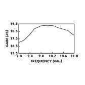 Fig. 7: The developed 4 × 4 element subarray measured gain.
Conclusion
The design of a complex multilayer 4 × 4 element antenna subarray with a corporate feeding network using a combination of commercial CAD tools (Ensemble, Touchstone and PCAAD) has been demonstrated. To make the design cost effective, aperture-coupled elements were developed using standard thin dielectric substrates and inexpensive foam to enhance the operational bandwidth. It has been shown that antenna CAD software can be used to obtain the antenna dimensions while the microwave circuit CAD software package can be used to optimize the feeding network, including microstrip discontinuities. The measurements of single elements are necessary to account for inaccuracies in the analysis and the manufacturing process. It has also been shown that the approach presented is predictive in nature and cuts the amount of time required to develop the multilayer subarray significantly. The developed antenna features approximately 10 percent return loss and gain bandwidth, making it a strong candidate for present and future wireless applications.
Acknowledgment
The work presented in this article has been supported by a collaborative research grant from Pohang University of Science and Technology, Republic of Korea. The Ensemble software package is a product of Boulder Microwave Technologies, Boulder, CO. Touchstone is a product of HP EEsof, Westlake Village, CA. PCAAD is a product of Antenna Design Associates Inc. RT Duroid and Ultralam are products of Rogers Corp., Chandler, AZ. The vector network analyzer used was the model HP8510C from Hewlett-Packard Co., Santa Rosa, CA.
References
- D.M Pozar, "A Review of Bandwidth Enhancement Techniques for Microstrip Antennas," Microstrip Antennas: The Analysis and Design of Microstrip Antennas and Arrays , Ed. D.M. Pozar and D.H. Schauber, IEEE Press, 1995, pp. 157-166.
- P.S. Hall and C.M. Hall, "Coplanar Corporate Feed Effects in Microstrip Patch Array Design," Proc. IEE , Pt. H., Vol. 135, June 1988, pp. 180-186.
- J. Huang, "The Finite Ground Plane Effect on the Microstrip Antenna Radiation Pattern," IEEE Transactions Antenna and Propagation , Vol. AP-31, No. 4, July 1983, pp. 649-653.
- J.F. Zurches, "The SSFIP: A Global Concept for High Performance Broadband Planar Antennas," Electronic Letters , Vol. 24, No. 23, Nov. 1988, pp. 1433-1435.
- J.S. Herd, "Modeling of Wideband Proximity-coupled Microstrip Array Elements," Electronic Letters , Vol. 26, August 1990, pp. 1282-1284.
- E. Levine et al., "A Study of Microstrip Array Antennas with the Feed Network," IEEE Transactions Antenna and Propagation , Vol. 37, No. 4, April 1989, pp. 426-434.
- Andrew A. Efanov and Hartwig W. Thim, "Corporate-fed 2 × 2 Planar Microstrip Patch Subarray for the 35 GHz Band," IEEE Antennas and Propagation Magazine , Vol. 37, No. 5, October 1995,pp. 49-51.
- Hyok J. Song and M.E. Bialkowski, "Design of a Microstrip Subarray for a Ku-band Squarial Antenna, Proceedings of the 5th Australian Symposium on Antennas , Sydney, Australia, February 1996.
- D.I. Wu and J. Huang, "CAD and Optimization of Circularly Polarized Microstrip Arrays," IEEE Antennas and Propagation International Symposium , Vol. 3, 1994, pp. 1840-1843.
- Boulder Microwave Technologies Inc., "Planar Antenna Design and Analysis Software," Microwave Journal , June 1996, pp. 96-100.