
This article reports the design and experimental characterization of an inverse Class E power amplifier (PA) with a finite DC-feed inductance. The output matching network is designed to transform the standard circuit impedance to the optimum device matching impedance with inherent harmonic suppression characteristics. The inverse Class E PA achieves a peak drain efficiency of 70.6 percent and power added efficiency (PAE) of 67.2 percent, with a gain of 13.2 dB, while providing 40.7 dBm output power at 2.87 GHz. It can produce output power greater than 38.2 dBm with a drain efficiency better than 60 percent across a 250 MHz bandwidth.
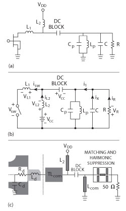
Figure 1 Generalized load network of an inverse Class E amplifier with finite DC-feed inductance ideal circuit (a) equivalent circuit (b) proposed circuit using transmission line (c).
The Class E power amplifier, introduced by N. Sokal and A. Sokal in 1975,1 has become very popular at RF and microwave frequencies due to its simplicity and high efficiency. As the dual to the classical Class E PA, the inverse Class E PA has several advantages. First, it operates with a lower peak voltage, which relaxes the high breakdown voltage requirement of the active device. Second, the internal parasitic inductance of packaged devices can be absorbed by the series inductor in the inverse Class E topology.2,3 There are some studies addressing this in the existing literature but almost all of the work assumes that the DC feed inductance has an infinite impedance.2-8 In practice, however, it is impossible to realize an RF choke with infinite impedance at the fundamental frequency and its harmonic components. Moreover, using a finite DC-feed inductance has the advantage of minimizing size, cost and complexity of the overall circuit. The effect of a finite DC-feed inductance on the performance of an inverse Class E amplifier is analyzed and the design equations are given in references Mury et al9 and Hietakangas et al.10 An additional capacitor is introduced in Mury et al9 to resonate with the finite DC-feed inductance at the second harmonic frequency.
This article presents an inverse Class E PA with finite DC-feed inductance which is resonant with a part of the parallel circuit capacitance at the fundamental frequency. The finite DC-feed inductance is realized as a short-circuited shunt stub. Theoretical expressions are derived for the circuit elements and the analysis is verified through simulation. For experimental validation, an inverse Class E PA employing a gallium nitride (GaN) high electron mobility transistor (HEMT) device is fabricated and measured.
INVERSE CLASS E CIRCUIT DESIGN
Fundamental Theory
Figure 1(a) shows the ideal equivalent circuit of an inverse Class E PA with finite DC-feed inductance. It consists of an active device as an ideal switch, a series inductor (L1), a parallel inductor (L2), a shunt resonant circuit (LpCp) tuned to the operating frequency, a compensation capacitor (C) and a load resistance (R). This circuit is usually analyzed based on preliminary assumptions.4 The output voltage and current are sinusoidal and are defined as
where ω = 2 π f0, f0 is the fundamental frequency, VR is the load voltage amplitude, φ is the initial phase, and G = 1/R is the load conductance.
From Figure 1 (b), it is seen that
When the switch is ON for 0 < ωt < π, the voltage on the switch is

At the same time, the current flowing through L1 can be written as
When the switch is OFF for π < ωt < 2 π the current
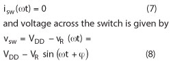
As is the case with other Class E amplifiers, it is possible to eliminate power losses during ON-to-OFF transition by providing the following collector-current conditions:
Applying the zero-current condition in Equation 9 gives
where -π/2 < φ < π/2 because VR > 0.
Applying the zero current-derivative condition of Equation 10 and using Equation 11 gives
and φ falls in the expected range for VR > 0.
As a result, the steady-state switch-current waveform for 0 < ωt < π and the switch-voltage waveform for π < ωt < 2π are
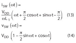
In the time domain, the switch current can be expressed in the form of a Fourier series as follows:
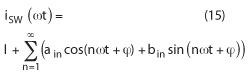
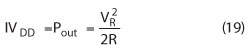
The DC supply current (I) can be found using Fourier transform equations and 4, 13 as
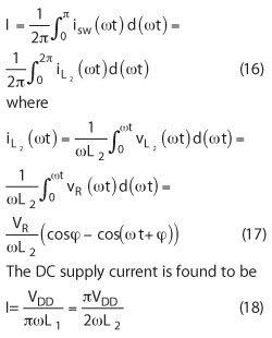
In an idealized inverse Class E mode of operation, there is no simultaneous nonzero voltage and current. That means that there is no power dissipation and the idealized collector efficiency is 100 percent. This implies that the DC power and fundamental output power are equal
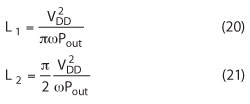
By using Equations 11-16, and PDC = I VDD, the optimum value of L1 and L2 can be obtained as
At the fundamental frequency f0, we can write 15 as
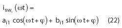
where ai1 and bi1 are de?ned as the Fourier coefficients of the switching current
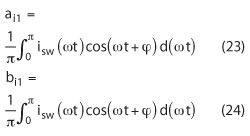
The coefficients ai1 and bi1 are found using Equation 13 to be
On the other hand, from Figure 1 (b), it is evident that
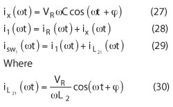
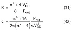
Using Equations 2, 11, 12, 22, 25-30, R and C can be obtained as
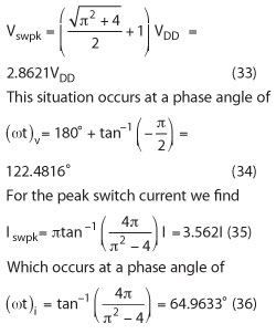
The peak values of the switch voltage (Vswpk) and switch current (Iswpk)can be determined by differentiating the corresponding waveforms given by Equations 13 and 14 and setting the results equal to zero, thus obtaining
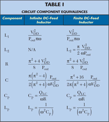
The optimum parameters are expressed as functions of a specific output power (Pout) and a given input DC voltage (VDD) at a specified operating frequency (fo) shown in Table 1. Table 1 also shows the optimum parameters of the classical inverse Class E topology.4
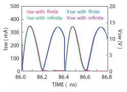
Figure 2 Current and voltage waveforms of the inverse Class E amplifier with finite or infinite DC-feed inductance considered.
Comparison
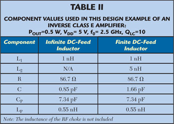
In this section, the simulated example of a 500 mW, 5 V Class E PA, operating at 2.5 GHz and having 10 percent bandwidth (QLC = 10), is provided as a means to verify the theoretical analysis. The values of the circuit elements for topologies with infinite and finite DC feed inductance are presented in Table 2. These quantities are computed based on the equations in Table 2. The active device is modeled as a switch which has 0.01 Ohms ON resistance (used because the Advanced Design System (ADS) simulation algorithm of the switch component does not allow 0 Ohms ON resistance) and 10 kOhm OFF-state impedance. Simulation results are shown in Figure 2. A sinusoidal voltage is used to drive the switch model used in the ADS simulation in such a way that the switch duty cycle is 50 percent. From the voltage and current waveforms, it follows that the waveforms for the circuit modeled with a finite DC-feed almost coincide with the ones for the circuit modeled with an infinite DC-feed. Theoretical results of the inverse Class E amplifier with infinite versus finite DC-feed topology are also given in Table 3, and compared to the simulation results. From Table 3, it is evident that the theoretical analysis is in good agreement with the simulation results. The same efficiency has been obtained from both power amplifiers.
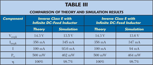
There are two advantages to using a finite DC-feed inductor (L2) as opposed to using an infinite one. First is that the size and complexity of the overall circuit are minimized. For this design example, an extra inductor (L2 = 5 nH) and a larger value of C (1.66 pF) are required for the inverse Class E topology with a finite DC-feed inductor (Table 3). Conversely, realizing a sufficiently high inductance to approach the infinite case would require greater circuit area. The second advantage is that the harmonic components are more thoroughly suppressed; resulting in higher output power and better drain efficiency. The parallel capacitance (C) can be divided into two parts; one part to compensate the phase angle error of the fundamental current, another to resonate with the finite DC-feed inductance at the fundamental frequency. The benefit of resonation at the fundamental frequency is better suppression at harmonic frequencies. This is indicated in the simulated results from Table 3 showing that the output power (464 mW) of the PA with finite DC-feed inductor is larger than the output power (462 mW) of the PA with the infinite DC-feed inductor.
Inverse Class E PA Using Transmission Line
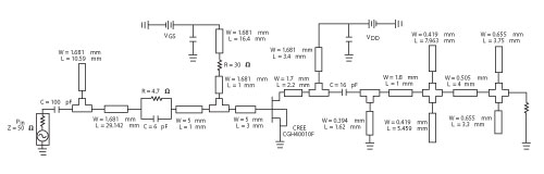
Figure 3 Full schematic of the proposed inverse Class E power amplifier.
For the experimental validation, a packaged GaN HEMT is used to replace the switch. The device cannot operate as an ideal switch due to the parasitic components caused by the package, interconnections and bond wires.6 Therefore, several internal parasitic components should be contained or compensated in the design procedure. Figure 1(c) depicts the proposed output equivalent circuit of the inverse Class E PA. The drain series inductance (Ld) is used as a part of L1 in Figure 1(a). A series transmission line (TLcom) is used as the tuning line to provide additional inductance because the value of Ld extracted by the model in reference Cabral et al11 is a little smaller than the optimum value of L1 calculated using equation 1. Meanwhile, Cd simply represents the sum of all capacitance seen at the drain, and is compensated by a short-circuit shunt stub since the inverse Class E PA cannot deal with the output capacitance of the device.
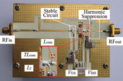
Figure 4 Photograph of the fabricated power amplifier.
Figure 3 shows the full schematic of the proposed inverse Class E PA. The finite DC-feed inductor (L2) is realized by a short-circuited shunt stub. The output network is designed to convert the standard 50 Ohm circuit impedance to an optimum matching impedance for the device of 83.9 Ohms using a simple L-type matching circuit. The lumped components are replaced by transmission lines using the Kuroda identity and the Richard transformation as explained in Mury et al.12 The parallel capacitance (C) is replaced by four open-circuited shunt stubs that are deliberately designed to accommodate the 2nd, 3rd, 4th and 5th harmonic terminations, dispensing with the need for a series-tuned LpCp circuit as in Figure 1(a). The input of the device is conjugately matched at the frequency of operation. The values of R1, R2 and C1 are obtained from the stability analysis based on S-parameter simulation in ADS.
FABRICATION AND MEASUREMENT
The proposed inverse Class E PA was designed and implemented using a 30-mil RO4350B substrate (εr = 3.5). The switching transistor is a Cree GaN HEMT power device (CGH40010F). Figure 4 shows the photograph of the fabricated amplifier.
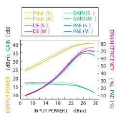
Figure 5 Simulated and measured output power, drain efficiency and PAE vs. input (f0 = 2.87 GHz, VGS = –3 V and VDD = 25 V).
Figure 5 shows the simulated and measured output power, drain efficiency, power-added efficiency (PAE) and gain of the proposed inverse Class E PA versus input power at 2.87 GHz. With the bias condition that VGS = −3 V, IDS = 50 mA and VDD = 25 V, the peak drain efficiency and PAE of 70.6 percent and 67.2 percent with a power gain of 13.2 dB were obtained at an output power of 40.7 dBm. The power gain of over 15 dB is maintained over a wide output power range. The measured harmonic suppression for the 2nd, 3rd, 4th and 5th harmonics are 32.5, 45.6, 42.8 and 60.6 dBc. The measured values are lower than those obtained by simulation (52.7, 57.97, 54.55 and 69.9 dBc) because the measured frequency (2.87 GHz) is shifted from the design frequency (3 GHz). The frequency shift is due to inaccuracies in the large-signal model of the transistor, as well as fabrication tolerances associated with the substrate and surface-mount technology passive components.
Figure 6 shows the simulated and measured output power, drain efficiency and PAE versus drain bias voltage at an input power of 27.5 dBm. It is worth noting that a high efficiency of over 65 percent is maintained over wide range of drain bias voltages (13 to 30 V), because a flat efficiency response versus drain bias is required for drain voltage modulations such as envelope elimination and restoration (EER).6
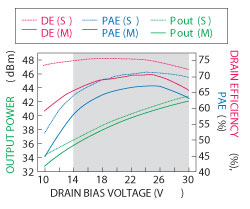
Figure 6 Simulated and measured output power, drain efficiency and PAE vs. drain supply voltage (Pin) = 27.5 dBm, f0 = 2.87 GHz and VGS = -3 V).
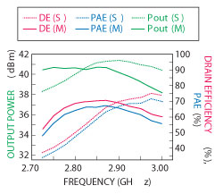
Figure 7 Simulated and measured output power, drain efficiency and PAE vs. operating frequency (Pin = 27.5 dBm, VDD = 25 V and VGS = -3).
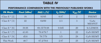
Figure 7 shows the simulated and measured output power and efficiency as a function of operating frequency at an input power of 27.5 dBm. Output power of greater than 38.2 dBm and drain efficiency better than 60 percent are achieved over a 250 MHz bandwidth (from 2.75 to 3 GHz). Compared to other inverse Class E power amplifiers (Table 4), the proposed inverse Class E PA exhibits similar levels of efficiency and output power.
CONCLUSION
In this article, we described the design of a GaN-based PA using inverse Class E topology with finite inductance and harmonic suppression. The design equations are given to determine the values of circuit elements. The peak drain efficiency of 70.6 percent, PAE of 67.2 percent with a gain of 13.2 dB is achieved at an output power of 40.7 dBm at 2.87 GHz. The measured results demonstrate the validity and advantage of the proposed GaN HEMT inverse Class E PA when used as a solution for high-power transmitters requiring high efficiency.
ACKNOWLEDGMENT
This work was supported in part by the National Basic Research Program of China (973 Program, No. 2010CB327506) and the National Natural Science Foundation of China (No. 61040061) and the Project supported by Hunan Provincial Natural Science Foundation of China (No. 11JJ2034).
References
- N. Sokal and A. Sokal, “Class E-A New Class of High-efficiency Tuned Single-ended Switching Power Amplifiers,” IEEE Journal of Solid-State Circuits, Vol. SSC-10, No. 3, June 1975, pp. 168-176.
- T. Brabetz and V.F. Fusco, “Voltage-driven Class E Amplifier and Applications,” IEEE Proceedings - Microwaves, Antennas and Propagation, Vol. 152, Issue 5, October 2005, pp. 373-377.
- T. Mury and V.F. Fusco, “Inverse Class-E Amplifier With Transmission-Line Harmonic Suppression,” IEEE Transactions on Circuits Systems I, Regular Papers, Vol. 54, Issue 7, July 2007, pp. 1555-1561.
- T. Mury and V.F. Fusco, “Series-L/Parallel-tuned Comparison with Shunt-C/Series-tuned Class-E Power Amplifier,” IEEE Proceedings in Circuit, Devices and Systems, Vol. 152, No. 6, 2005, pp. 709-717.
- W. Saito, T. Domon, I. Omura, M. Kuraguchi, Y. Takada, K. Tsuda and M. Yamaguchi, “Demonstration of 13.56-MHz Class-E Amplifier using a High-Voltage GaN Power-HEMT,” IEEE Electron Device Letters, Vol. 27, Issue 5, May 2006, pp. 326-328.
- F. You, S. He, X. Tang and X. Deng, “The Effects of Limited Drain Current and On Resistance on the Performance of an LDMOS Inverse Class-E Power Amplifier,” IEEE Transactions on Microwave Theory and Techniques, Vol. 57, No. 2, February 2009, pp. 336-343.
- Y.S. Lee, M.W. Lee, S.H. Kam and Y.H. Jeong, “A High-Efficiency GaN-Based Power Amplifier Employing Inverse Class-E Topology,” IEEE Microwave and Wireless Components Letters, Vol. 19, No. 9, September 2009, pp. 593-595.
- S.H. Kam, M.W. Lee and Y.H. Jeong, “A High-efficiency Inverse Class-E Power Amplifier Using Double CRLH-TL for 3.5 GHz WiMAX Applications,” Proceedings of the Asia-Pacific Microwave Conference, December 2011, pp. 514-517.
- T. Mury and V.F. Fusco, “Analysis of the Effect of Finite DC Blocking Capacitance and Finite DC Feed Inductance on the Performance of Inverse Class-E Amplifiers,” IEEE Proceedings - Circuits Devices and Systems, Vol. 153, No. 2, pp. 129-135, 2006.
- S. Hietakangas, J. Typpo and T. Rahkonen, “Integrated 1.6 GHz, 2W Tuned RF Power Amplifier,” 26th Norchip Conference, November 2008, pp. 176-179.
- P.M. Cabral, J.C. Pedro and N.B. Carvalho, “Nonlinear Device Model of Microwave Power GaN HEMTs for High Power-Amplifier Design,” IEEE Transactions on Microwave Theory Techniques, Vol. 52, No. 11, November 2004, pp. 2585-2592.
- T. Mury and V.F. Fusco, “Transmission Line Matching Effects on the Performance of Shunt-C/Series-tuned and Series-L/Parallel-tuned Class-E Amplifiers,” 2005 Asia-Pacific Microwave Conference Proceedings, December 2005, pp. 565-1568