
Designing components and subsystems for use at RF and microwave frequencies is no longer achieved with a ball-peen hammer, epoxy filler and paint. Today’s engineers are required to hit performance specifications in a smaller footprint, using new materials to reduce cost and weight and under significant time-to-market pressure. This new norm has led to the widespread use of RF/microwave centric design and EM analysis tools. These software products are under significant pressure to improve their speed, capacity, accuracy and time-saving automation. The following contributions from many of the industry’s leading design software vendors reflect the state of software tools in 2013.
Agilent
Engineers require design flow integration because today’s RF/MW designs themselves have become more integrated. The RF modules inside popular wireless consumer products contain multiple ICs on a small printed circuit board (PCB) carrier or laminate connected to the ICs with wire bonds or solder bumps and are covered in a compound mold or package. When designing these RF modules, engineers use a variety of design software to simulate and fabricate the individual components, as well as the completed consumer wireless device. Each tool typically performs an individual function, such as schematic, IC layout, PCB/laminate layout, circuit simulation, layout verification, planar electromagnetic (EM) simulation, 3D EM simulation or packaging. While some Electronic Design Automation (EDA) vendors do offer tools with multiple functions, companies often purchase tools from several vendors to have a complete RF module flow. In response, EDA vendors have developed design flow integration solutions based on point-to-point links between tools. This approach inherently has the potential to corrupt user design and make round trip design iteration an even bigger challenge.
A preferred approach would maintain the integrity of the users’ design data by architecting the design software so that translation, migration or conversion of the data to another format is never necessary. This idea began several years ago with the concept of an open, industry standard database on which design software is built. Today, enterprise EDA vendors, like Cadence, Synopsys and Mentor Graphics, are using the same industry standard, open database structure for schematic and layout design data; they are also developing layout verification tools that operate on this customer design data.
While this concept was originally created for single technology ICs, Agilent extended it to multiple, heterogeneous technologies, including IC, laminate/PCB, packaging and 3D solid model technologies. With the help of several of its customers who are industry-leading RF and microwave suppliers, Agilent embarked on a multi-year effort to re-engineer its Advanced Design System (ADS) and EMPro software platforms to incorporate this expanded concept. The result is the next generation of these platforms—ADS and EMPro 2012.
A simple, but compelling example of the design flow integration now present in these tools is the ability for EMPro and ADS to directly share design data. A 3D solid model created in EMPro can be directly opened in ADS for Finite Element Method (FEM) simulation in a larger multi-technology design. Freescale Semiconductor took advantage of this concept to develop a new discrete design methodology, dramatically improving its power amplifier design flow. A webinar is available at mwjournal.com/ADSFreescaleWebinar.
ANSYS
The new 3D electrical layout interface for ANSYS HFSS allows engineers to easily create designs consisting of fully parametric planar stackups, via padstacks, transmissions lines and other planar structures and transitions with a few button clicks. In addition, the new interface has a simplified boundary assignment methodology and automated excitation assignments which reduce the engineering and simulation setup times. While the user interface and model creation has been greatly simplified, the solution is still generated by the trusted HFSS solver. This enables true 3D electromagnetic field analysis of key design parameters, including trace thicknesses, etching, bondwires, solder balls and solder bumps in a robust, reliable, and highly accurate design and simulation flow.
The new functionality integrates with existing ECAD design flows and can import geometry from Altium, Cadence, Mentor Graphics, Zuken, and ODB++ compatible databases allowing full or partial designs to be imported directly. Specialized integration with Cadence is also included so users of Cadence software can set up ready-to-solve chip, package and PCB simulations directly from Allegro® Package Designer, Allegro PCB Designer, SiP Digital Layout, or Virtuoso® Analog Design Environment for analysis in HFSS. All the necessary HFSS set-up steps – geometry and net selection, material properties, excitations and boundary conditions – are completed in the Cadence software and transferred to HFSS for solving the electromagnetic field and S-parameters via a single click.
ANSYS also provides direct integration of Synopsys® HSPICE® through ANSYS Designer. Using ANSYS Designer and its tight integration with HFSS solver technology, engineers have a design platform where the ANSYS best-in-class electromagnetic field solver technology HFSS, Q3D Extractor, SIwave and the gold standard transient circuit simulator HSPICE can operate from a single interface. This results in the Gold Standard design platform for signal- and power-integrity analysis. With ANSYS Designer at the core of this platform high-speed component designers can analyze 3D EM behavior of advanced electronic systems, including gigabit communications channels and high-speed wireless systems. Users can combine S-parameters, w-elements, HSPICE, HSPICE encrypted, IBIS and IBIS-AMI models directly as schematic components allowing them to seamlessly integrate with behavioral, circuit and GHz-accurate interconnect models in a unified schematic desktop.
AWR
AWR’s EM simulation software tools, like Analyst™ 3D finite element method (FEM) EM simulator, AXIEM® 3D planar EM simulator and EM Socket™ technology introduced in 2003, are now seamlessly integrated within their Microwave Office® (MWO) circuit design software to address RF/microwave and wireless systems that are being designed into shrinking footprints and/or alternative processes such as GaAs and GaN. This allows MWO circuit designers to directly access EM simulation within a single design environment. This integration allows designers to easily transition from system to circuit to EM analysis automatically, addressing design functions such as drawing 3D shapes, extrusions, port setup and meshing/convergence tweaks, not to mention importing and exporting either CAD and/or resulting S-parameter files across vendor environments.
The AXIEM tool addresses 3D planar applications such as RF printed circuit boards (PCB) and modules, low temperature co-fired ceramic (LTCC), monolithic microwave integrated circuit (MMIC) and RFIC designs. By delivering EM analysis as an integral part of the design flow, Axiem benefits designers by helping to diagnose issues early, thereby shortening the design process. It does this by pulling from the schematic/layout and automatically understanding the circuit hierarchy and nuances necessary from EM so that ports, frequencies, convergences criteria, etc. are all pre-set for the user such that a single button click runs the EM simulation and analysis. Analyst provides similar functionality for EM analysis of 3D interconnect in chip/board/module designs. Analyst eliminates the need to launch a third party drawing and simulation tool, operating directly from Microwave Office with a single mouse click. Layout setup and drawing are simplified through automatic simulation settings and preconfigured 3D parametric cells (Pcells) that eliminate manual setup and drawing tasks.
What AXIEM and Analyst really have in common goes beyond the fact that they are both powerful yet easy to use and intuitive EM simulators. They embrace the modular approach that AWR has built from day one within its AWR Design Environment™ framework using the EM Socket interface. The concept is, quite simply, the ability to use one or multiple EM tools, from method-of-moments (MoM) to finite difference time-domain (FDTD) to full FEM or even FIT as an integral part of the design flow. This is a critical requirement for circuit designers (MMIC, MIC, RFIC, RF PCB, microwave modules, et al) and yet the essence of what methodology would be best for each individual design task (fastest, most accurate, etc.) is left to the discretion of the user or customer or industry.
Cadence
The Allegro Sigrity® signal integrity (SI) product integrates advanced EM analysis for PCB and IC package design in a constraint-driven design environment. The Allegro physical implementation tools enable PCBs, single die packages or stacked die packages to be designed and prepared for manufacturing.
Many products are being implemented using lower voltages with faster data transfers. In years past, SI tools focused on the signal path and assumed that the current would return on an ideal power/ground return path. At slower speeds and larger voltage swings, it was relatively safe to assume ideal power and ground, and to build in a small amount of margin for noise on the planes and timing push-out due to simultaneous switching output (SSO) noise. Today, however, assuming ideal power and ground is a risky proposition as the ground plane discontinuities and simultaneous switching noise (SSN) effects now consume a much larger portion of both the signal quality and timing budgets.
Allegro Sigrity SI products provide a power-aware signal integrity environment for multi-gigabit SerDes and DDR interface design. The SI tool suite is constructed such that base level analysis using 2D boundary element method (BEM) and finite element method (FEM) field solvers provides quick results using first-order analysis techniques such as ideal power and ground and uncoupled via modeling. Later in the design process, engineers can call on detailed power-aware SI analysis. The power-aware technology includes advanced field solvers for modeling interconnect used in high-frequency signaling. The hybrid (2D/3D) and full-wave solvers model signal, power and ground in a fully coupled manner. A SPICE-based simulator provides transient circuit-level analysis results from circuits that span across chip, package and board. All the effects of SSN are considered. The highly automated post-analysis waveform processing and report generation verify timing closure on DDR interfaces and ensure electrical specification compliance on SerDes interfaces.
The die-to-die system-level analysis is largely enabled through the intelligent combination of circuit analysis and EM analysis. Circuit-level analysis is used to connect the interconnect models. The models can be an extraction of individual pieces such as traces, vias, pads and wirebonds, or they can be s-parameter data that is collected from a test bench using test and measurement equipment such as a vector network analyzer (VNA). EM analysis (both 2D and 3D) is applied during the extraction of signal interconnect while 3D EM analysis handles power planes and shapes. The circuit and the 3D EM analyses are merged into one fully coupled model. All local and global SI and PI effects are considered by this combined circuit/EM analysis approach.
For ultra-high-frequency designs, extraction of interconnect is commonly accomplished with 3D full-wave EM techniques. To enhance accuracy, the hybrid solver technology is supplemented with a 3D FEM field solver within Allegro Sigrity SI tools. 3D EM is commonly used to extract interconnect of multi-gigabit channels, breakout regions for dense packages and connectors or for high-density interconnect (HDI) via technology commonly used in high-end consumer devices.
Tunable cavity filter. Photo courtesy of COMSOL.
COMSOL
COMSOL Multiphysics software provides 38 application-specific modules in the electrical, mechanical, fluid and chemical disciplines so that COMSOL users can simulate their applications with a multiphysics approach. The six modules developed for the electrical engineering discipline include: the AC/DC Module, RF Module, Wave Optics Module, MEMS Module, Plasma Module and Semiconductor Module. The RF Module models the propagation of electromagnetic waves in and around structures. The new Wave Optics Module accurately simulates optical systems with geometric dimensions much larger than the wavelength. When analyzing electrical devices and circuits, the AC/DC Module allows users to go beyond conventional analysis by providing a simulation for a mixed system of lumped and high-fidelity models.
A particular strength of COMSOL Multiphysics is its ability to combine any physics effect with any other, such as RF heating, mechanical stress and deformation effects – all crucial components in electrical applications. In addition to its multiphysics capabilities, COMSOL simplifies the design process with a single, intuitive modeling and simulation environment. From within this interface, the design flow process of a product or design can be integrated with COMSOL Multiphysics using the LiveLink™ products, which allow for interfacing between COMSOL and other simulation and CAD software.
For example, a Tunable Cavity Filter includes a piezo actuator that is used to control the size of a small air gap in a cavity filter which tunes the resonant frequency. Results show the S-parameter as a function of the frequency and total displacement of the actuator. Cavity filters are used in wireless products, RF and satellite applications.
In a second example, a Self-Focusing Laser Beam uses a model of a self-focusing Gaussian beam developed using the Wave Optics Module (this is important in the design of high-power laser systems). The simulation demonstrates 3D nonlinear wave propagation and the distribution of the index of refraction within the lens.
CST
Cst Studio Suite® provides a smooth workflow for the whole product design cycle including tools for importing and exporting CAD and EDA files in numerous industry standard formats. However, since models used in field simulation have to fulfill special requirements, models created with CAD software are often not suitable for simulation directly, perhaps because they are too detailed or contain flaws and corrupted elements. These are dealt with using shape-healing tools to convert CAD data into a simulation-ready model. To process data, which are often layered, 2-dimensional structures, from EDA software, CST can create 3D models based on stack-up, via and bondwire information. The ability to parameterize imported models enables optimization and sensitivity analysis even if the geometry was not originally generated in CST STUDIO SUITE.
CST STUDIO SUITE provides a template-based post-processing system which automates using simulation results to calculate additional user-relevant data. Built-in optimizers are included as a standard feature of the software. The software also includes links to a number of specialist products, such as Optenni Lab for matching circuit tuning and EMIT for co-site interference analysis. These additional products can read models and fields from CST STUDIO SUITE simulations and use them as the basis of further calculations, without the need to start from scratch. Engineers can also use their own VBA macros or MATLAB code to fully control the software and analyze the data to support their own unique requirements.
Complex systems may contain several elements that are each suited to a different solver. One such example is a satellite dish, where the feed network is well suited to a frequency domain solver, the feed antenna is best simulated with a time domain approach and the reflector dish needs an integral equation solver. CST’s “Complete Technology” approach offers on demand access to all these simulation methods in a single design environment. System Assembly and Modeling (SAM) allow users to build their own simulation flow within CST STUDIO SUITE. Rather than using a single 3D model, the antenna can be built as a series of components linked using either S-parameters or near or far field sources. The simulation sequence can be set up to run automatically, with the result calculated at each step being used as the basis for the next.
Another use of SAM is in multiphysics analysis. Field losses generate heat and this heat can damage materials or detune the structure by causing thermal expansion. Investigating this effect means carrying out four simulations: an initial full-wave electromagnetic (EM) simulation to calculate the field losses, a thermal simulation to calculate the heating effect of these losses, a structural mechanics simulation to calculate the thermal expansion and a final EM simulation to calculate field behavior in the new, deformed structure. These tasks can be set up as a sequence and evaluated automatically to speed up such multiphysics flows.
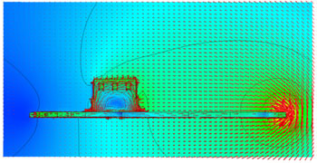
Magnetic fields coupling to a connector on a mobile device PCB. Photo courtesy of FEKO.
FEKO
Ever-increasing component and trace densities compounded with higher clock speeds result in electromagnetic interactions that may be difficult to predict. With the 3D electromagnetic simulator FEKO, design engineers have access to a host of numerical technologies that enable them to avoid problems before they occur. For example, the geometry of a design layout can be imported (e.g., using DXF or Gerber formats) into FEKO, where the various 3D solvers can be applied to calculate cross talk and radiated fields. R, L and C elements can be included as lumped elements, while more complex circuits and networks are added using the schematic editor. By including circuits in the electromagnetic simulation, the design engineer performs a more comprehensive analysis in FEKO than in a stand-alone simulator. The Spice co-simulator is included with FEKO at no extra cost. Many design parameters are obtained from FEKO, including voltages, currents and S-parameters. The latter can be exported in Touchstone format for inclusion in system simulators. Alternatively, measurement data can be imported directly into FEKO for comparison purposes.
FEKO is especially valuable to investigate optimum strategies for component placement, cable routing, shielding, and to design antennas, including on-chip and on-package antennas. Inherent parametric modeling capabilities are available, enabling geometry to be created and defined in terms of variable dimensions. These variables are passed to an automated optimization engine so that the geometry can be modified to achieve specific performance goals. Different optimization technologies are available including the Generic Algorithm (GA) method. GA is well suited to solve multiple-variable, multiple-goal problems, as it is renowned for finding the best configuration. Automated optimization is ideal for both coupling and radiation applications.
Integration of third-party tools further simplifies antenna design: Antenna Magus offers antenna synthesis capabilities for a large number of antenna types, while Optenni Lab offers fast matching-circuit design, including broadband, multi-band and multi-port matching.
Magnetic fields coupling to a connector on a mobile device PCB and the induced currents that flow on PCB. The increased coupling can be visualized in between the battery and PCB.
PCB design. Photo courtesy of IMST.
IMST
IMST develops RF components in combination with its EMPIRE XCcel 3D EM field solver. Based on the 3D Finite Difference Time Domain method, the software offers an easy-to-use graphical user interface with extensive layout capabilities, yield analysis and smart optimization algorithms as well as intelligent remote control to distribute simulation jobs efficiently in LAN-networks. In addition, EMPIRE has been highly optimized with respect to simulation speed in order to achieve fast results using off-the-shelf workstations. By using a state-of-the-art software controlled workflow algorithm for distributing the simulation job among various CPUs, a speed of 5 GCells/s can be achieved today on a standard dual CPU machine. Such speeds enable the designer to run a huge number of parameter variations of planar circuits or to analyze highly complex multi-layered modules in almost no time at all.
The extreme high speed is also the key for the next level of design integration. Up to now the conventional design flow was to embed full 3D EM simulation results of passive components and small circuit parts in co-simulations using a separate circuit simulator. This causes inaccuracies due to the limited modeling validity, especially if the components are spaced closely together. However, today it is possible with 3D EM simulations to analyze whole passive circuits for a specified frequency range within minutes.
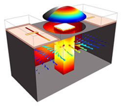
In order to account for active devices, RLC-Elements and S-parameter files can be embedded into the 3D EM simulation. This is done using a schematic entry of symbols and defining virtual connections to the internal ports. The figure shows a design example of an LNA using EMPIRE where two transistor measurements are included as 2-port S-parameters set. SMD elements are modeled as 3D structures with internal ports to allow tuning of the element values. Such a design can be carried out without using an additional circuit simulator within a very short time frame. All parameters of the design can be tuned and used as input for different optimizers in EMPIRE. The final layout can be checked (e.g., automatic connectivity check) directly before exporting it to a variety of formats (DXF, Gerber, GDS).
Intercept Technologies
In contrast to the “all-in-one” solution that tries to span the entire design cycle, Intercept favors a multi-vendor approach to integrate PCB design flow with simulation and analysis software. Whenever possible, Intercept’s interfaces are made bidirectional so that data can pass freely to and from design, layout, modeling and simulation. The company’s Pantheon product currently offers bidirectional interfaces to and from AWR’s Microwave Office, HFSS and ANSYS Designer.
Taking the customers’ needs a step further, Intercept is currently developing a method by which vendor-approved RF models can be created and modified parametrically using a direct link to Microwave Office and Agilent ADS library models. This allows models placed into Intercept’s Pantheon layout software to be simulation-ready at all times. By offering enhanced communication between RF and PCB layouts, there are fewer steps to design completion and fewer interruptions in the work being done in either application. In line with this, Intercept is working toward future developments with RF simulation and modeling vendors that will provide the simulation directly within Pantheon, eliminating the need for data transfer and further error-proofing processes for designers and engineers.
Mician
Advanced RF simulation software is a substantial investment and an exact computer model of an RF component is expected to generate exact results, just as measured. For more accurate results, better models need to be built using full wave EM simulation software based on various techniques. FEM, MoM and FDTD are versatile methods with virtually no limitations in complexity but they require fast computers with a substantial amount of RAM. Large, complex structures significantly increase CPU time, making optimizations almost impossible. Mode Matching has low CPU and RAM requirements and simulates complex structures fast and accurately, provided eigenvalues for all geometries are known. Boundary Contour Mode Matching (BCMM) has proven to be a suitable replacement for certain 3D FEM applications.
Hardware and software advancements support accurate simulation of highly complex assemblies, but there is no all-in-one design software on the market. Modeling requires in-depth knowledge of drafting or model building tools and solver settings. The more flexibility and options the product offers, the more familiar the user needs to be with the product or its strength will become a weakness. GUI’s become overwhelming for the novice and the casual user.
Hybrid solvers such as MICIAN µWave Wizard™ combine different solvers for increased simulation efficiency, overcoming the limitations and shortcomings of single solvers. The modal port concept of µWave Wizard facilitates dissecting complex structures into more fundamental sub-structures. The program assigns each sub-structure to the most suited of the built-in solvers (MM, 2D FEM or 3D FEM), allowing it to operate within its comfort zone with little need for user interference. Homogeneous cylindrical structures of finite length will only be treated as multimode transmission lines, leading to a drastic reduction of computation time. Afterward, results from individual solvers are cascaded multimodal to generate S-parameters of the composite structure.
By breaking complex structures down into basic sub-circuits or components such as irises, geometries can be parameterized for optimization or tolerance studies. Sub-circuits excluded from optimization are only simulated once and their respective S-parameters temporarily stored for subsequent cascading with those of the optimized circuits. Additional advantages are breakpoint analysis capability, allowing for separate S-parameter analysis of components or subsystems within a complex assembly and ease of use through convenient composition of complex structures either by drafting tool or through use of parameterized library elements.
MiG
Converting synthesized prototype values reliably into actual physical filters is often a challenge. MiG’s latest hybrid electromagnetic (EM) computer-aided design (CAD) technology implemented in its CAD and optimization tool WASP-NET meets this demand by streamlining the filter design flow and reducing overall design time. As the first step in advanced filter design flow integration, the coupling (or M-) matrix approach supports synthesis of practically any kind of filter characteristics on a prototype level and selection of the appropriate topology for adequately placing the important cross-couplings. In this way, the best suited topology for a given filter problem can be found.
In the second design step, synthesized M-matrix parameters are converted into an initial approximation of physical dimensions by applying 3D EM simulations stepwise for isolated structure parts – e.g., for inter resonator couplings between two resonators, for external couplings between in-/output ports and for cross-couplings between two resonators.
In the commonly used filter design flow, a third design step is applied, during which lookup tables or parameter plots are generated from the EM data of step 2, relating isolated physical dimension data to circuit level parameters. The design of the total filter is then commonly carried out by optimization on this circuit level based on different modeling techniques, such as lumped element, distributed line, neural network or space mapping approaches, and by executing sporadic correction loop calculations applying EM simulators. The last design step applies EM solvers to analyze the total filter, making some final stepwise corrections. Direct EM level optimization – though very desirable – is still judged hitherto taking an enormous amount of time and is therefore considered impractical.
MiG’s filter design flow includes a new integrated M-matrix designer that makes step 3 unnecessary and carries out design steps 1 and 2. Recent advances in the fast hybrid mode-matching/multi-solver 3D EM CAD engine of WASP-NET enable filter designers to apply the last, final EM level in filter design flow directly and efficiently after design step 2. The filter design flow is drastically simplified and reduced concerning both design time and complexity. No time consuming, and often cumbersome, interim circuit level mapping is necessary, and the filter can be optimized directly on the EM level.
Remcom
In its most recent release, Remcom offered users a breakthrough in FTDT-based electromagnetic simulation performance with MPI + GPU technology and unlimited memory support for the company’s XFdtd® Electromagnetic Simulation Software (XF7). By combining Message Passing Interface (MPI) technology with XStream® GPU Acceleration, multiple high-performance graphical processing units (GPU) in separate computers can be linked together, resulting in tremendous increases in processing speed and available memory. Complementing this technology with unlimited memory support gives XF7 the robustness to simulate massive problems exceeding billions of cells.
The new speed performance enables users to simulate increasingly complex scenarios in a reasonable timeframe. A growing number of designers have exhausted the amount of GPU RAM available for use in a single machine but still wish to grow the complexity of their models. Extending the GPU capabilities to leverage additional cards through clustering creates a solution with limitless potential. The MPI + GPU can dramatically cut your simulation times by orders of magnitude.
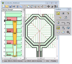
Stack up manager. Photo courtesy of Sonnet.
Sonnet
The Blink™ passive device modeling system automates the Sonnet planar electromagnetic (EM) simulator setup and design flow in the Cadence Virtuoso environment to easily simulate spiral inductor, balun, transformer, and capacitor designs on silicon. In these design flows, Blink and Sonnet can work with process design kit (PDK) specific information, such as stack ups, metal properties, and via properties. Starting from operation completely within Cadence, users can export Sonnet EM simulations outside of the Cadence environment where Sonnet can run completely stand-alone. This flexibility of design flow allows Sonnet to connect different design flows together.
For integrated circuit designs incorporating RF functionality, design work often starts in Agilent’s ADS. The Sonnet EM simulator installs in ADS as a design kit and operates completely from within the ADS environment. Sonnet EM simulations can be exported from ADS to stand-alone Sonnet simulation, and already-existing Sonnet stand-alone designs can be brought into ADS. Thus designs and design flows that were originally disparate, an RF design flow in ADS, and an analog mixed-signal design flow in Cadence Virtuoso can be reconciled and connected with EM simulation analysis and layout geometry using Sonnet.
Another advantage of interconnecting designs and design flows using Sonnet is the commonality of popular functions like the stack up manager. Sonnet’s new version 14 provides technology layers and a stack up manager that displays the dielectric and metal layers. Users can click on a chosen dielectric or metal layer or via to navigate through stack ups with dozens of layers. The stack up manager feature also appears with Sonnet in Cadence Virtuoso and Agilent ADS.
Tech-X
The VSim family of commercial products from Tech-X are based on the Vorpal simulation engine, a flexible electromagnetic, particle, and plasma physics software application initiated in 2001 for government applications. In the early years of its development, it was used to meet the needs of a variety of challenges for the federal government including plasma acceleration, accelerator cavity modeling and magnetic fusion studies. VSim offers a diverse range of examples, macros and the VSimComposer interface to the Vorpal simulation engine together with embedded analysis tools. The new Vorpal 6.0 features customized VSim packages for the simulations of microwave devices and plasma discharges and increased features for electromagnetic simulations. VSim for Microwave Devices (VSimMD), includes a full suite of electromagnetic and particle modeling features for magnetrons, klystrons, gyrotrons, TWTs and similar devices and is optimized for solving large problems on parallel computing hardware.