
Advances in Receiver Front-end and Processing Components
Ted Heil, Bill Roehrich and Jack Hakoupian
MITEQ Inc.
Hauppauge, NY
Since the introduction of radar, the goal of the radar systems engineer has been to improve overall range and accuracy performance. Radar range is defined in the classical radar equation, as shown in Skolnik's Introduction to Radar Systems :
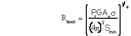
where
Rmax = maximum range
Pt = transmit power G = antenna gain s = isotropic target area Smin = minimum detectable signal Ae = receive antennaís effective area
There are several approaches an engineer can take to improve range performance, including increasing the transmit power, increasing the antenna gain, increasing the effective area of the receive antenna and reducing the minimum detectable signal.
In reality, Smin is a statistical value based upon the probability of detection PD and the probability of false alarm PFA. As with any receiving system, the signal must compete with the excess thermal noise generated by the receiver. Reducing this noise would result in a reduction of the minimum detectable signal and, therefore, an improvement in the overall range of the radar.
The excess thermal noise generated in the receiver is characterized by a parameter called noise figure. The noise figure is the ratio of the additive receiver-generated noise to the thermal noise floor present at the input (ñ114 dBm/MHz). Low noise amplifiers (LNA) are used at the input to set the noise figure for the entire receiver chain, as shown in Figure 1 .
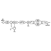 Fig.1: A typical radar receiver front end.
Early LNAs
The earliest form of LNAs was a parametric amplifier, which utilized diodes and high frequency sources at specific pump frequencies to provide low noise gain at the desired C-band (5.4 to 5.9 GHz) and X-band (8.5 to 9.6 GHz) frequencies. These amplifiers were sometimes cooled cryogenically for further improvements, but even uncooled, they were extremely large, expensive and unreliable.
As GaAs FET semiconductor development advanced in the late 1960s and early 1970s, component engineers started to develop LNAs that would ultimately compete with the parametric amplifier hold on the radar market. Although at the time the noise figure performance of these solid-state amplifiers could not approach that of parametric amplifiers, the size, cost and reliability improvements made them clear competitors. Table 1 lists the design achievements of LNAs over the last 20 years.
|
Table I: LNA Desig History | |||
|
|
Device |
Noise Figure (dB) | |
|
|
|
C-band |
X-band |
|
Parametric amplifier |
|
0.5 |
|
|
Solid-state amplifiers* |
|
|
|
|
1975 to 1980 |
GaAs MESFET |
2.0 |
3.5 |
|
1980 to 1985 |
GaAs MESFET |
1.3 |
1.7 |
|
1985 to 1988 |
GaAs HEMT |
1.1 |
1.5 |
|
1992 |
GaAs PHEMT |
0.8 |
1.3 |
|
1994 |
GaAs PHEMT |
0.5 |
0.7 |
|
*Coaxial input, do not include input isolators or limiting diodes |
|
|
|
The LNA Design Approach
In using GaAs FETs for low noise designs, the input to the FET (the gate) must be matched to the impedance of the preceding system element. The impedance standard had been set at 50 ohms long ago. However, the gate circuit of a FET presents a much higher impedance that changes with frequency. Therefore, matching circuits are required to transform the input impedance of the FET to 50 ohms. In designing this circuit, a trade-off must occur between two parameters: power and noise. It is inherent in the FET that a network that provides the best match for noise figure will not yield a simultaneous best match for power conditions (low SWR). To approach the best compromise, a complicated matching network is required, which typically results in large losses before the transistor, further degrading the overall noise figure. From the early days of solid-state LNA design, input isolators were used to accommodate the power matching conditions so the designer could concentrate on matching for low noise, as shown in Figure 2 .
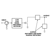 Fig. 2: An isolator input design.
More recently, a technique called lossless feedback has been implemented as a result of assembly technique advances using thin-film hybrid MIC construction. This approach, shown in Figure 3 , requires the manipulation of the microminiature bond wires and die components to create matching elements in a series feedback path. At this point, matching is considered lossless because these elements do not affect the input path of the transistor. Using this technique, a nearly perfect trade-off of a simultaneous noise and power match can be achieved without an input isolator. With lossless feedback, the net result is further reductions in LNA noise figures and, therefore, improved system performance.
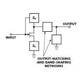 Fig.3: A lossless feedback design.
Input Power Considerations
Another design consideration relates to handling the leakage power from the transmitter. Since most radars utilize a common transmit and receive (TR) feed, the receiver is subject to extremely high input powers. High power limiters are used to protect the input of the receiver from these power levels. However, the limiters have a leakage current that can still harm the sensitive receiver components.
Typical levels from TR limiters are 5 W spike leakage and 50 mW flat leakage. The GaAs MESFETs used in low noise input stages years ago could handle these input levels. However, both the high electron mobility transistors (HEMT) and pseudomorphic HEMTs (PHEMT) will be damaged permanently at these leakage powers. Typical characteristics of an LNA manufactured in 1985 and using a MESFET input stage, an input isolator, and a waveguide input and SMA output are listed in Table 2 . If an LNA with HEMT or PHEMT inputs is to be used with these maximum input levels, then additional protection must be incorporated inside the amplifier. This protection comes in the form of a solid-state PIN diode limiter. The limiter is mounted before the low noise gain stage and will provide a maximum output power under both spike and flat leakage conditions that will not damage the amplifier.
|
Table II: Typical Performance of an LNA with a MESFET Input Stage | |
|
Operating frequency (GHz) |
5.4 to 5.9 |
|
Gain (vs. temp. & freq.) (dB) |
20 to 22 |
|
Gain flatness (peak-peak)(dB) |
0.5 |
|
Noise figure (max) (dB) |
1.5 |
|
Input/output SWR |
1.25 |
|
Output power |
0 |
|
Maximum input power (W) |
5 peak |
Using a PIN diode limiter is not without consequence. The additional loss of the device will degrade the noise figure by approximately 0.2 dB in C-band and 0.5 dB in X-band. It should also be noted that some radar systems engineers are concerned about the reflected power from the limiter under the spike leakage conditions. These engineers sometimes specify input isolators to be used in conjunction with the limiters to prevent this energy from being reflected back into the TR circuit. Table 3 lists LNA performance that is available today.
|
Table III: Current LNA Performance | ||||||
|
C-band (5.4 to 5.9 GHz) | ||||||
|
|
|
|
Max Signal (W) | |||
|
Model |
Design |
FET |
Peak |
CW |
Input |
Noise |
|
AMF-2S-5459-09-WG |
isolator input |
MESFET |
5 |
0.05 |
1.25 |
1.5 |
|
AMF-2F-5459-09-WG |
feedback |
PHEMT |
50 |
1 |
1.25 |
0.9 |
|
AMF-2F-5459-15 |
feedback |
PHEMT |
0.2 |
0.03 |
1.25 |
0.7 |
|
JS-04000800-05 |
feedback |
PHEMT |
0.2 |
0.03 |
1.5 |
0.5 |
|
AFS3-05400590-06-8P-4 |
feedback |
PHEMT |
0.2 |
0.03 |
1.25 |
0.6 |
|
AFS3-05400590-06-L-4 |
feedback |
PHEMT |
50 |
1 |
1.5 |
0.8 |
|
X-band (8.5 to 9.6 GHz) |
|
|
|
|
|
|
|
|
|
|
Max Signal (W) |
|
|
|
|
Model |
Design |
FET Peak |
CW |
Input |
Noise |
|
|
AMF-3S-8596-20-L |
isolator input |
PHEMT |
50 |
1 |
1.25 |
1.7 |
|
AMF-3F-085096-11 |
feedback |
PHEMT |
0.2 |
0.03 |
1.25 |
0.9 |
|
JS-08001200-07 |
feedback |
PHEMT |
0.2 |
0.03 |
1.5 |
0.7 |
|
AFS3-08500960-09-8P-4 |
feedback |
PHEMT |
0.2 |
0.03 |
1.5 |
0.9 |
|
AFS3-08500960-11-L-4 |
feedback |
PHEMT |
50 |
1 |
1.5 |
1.1 |
Conclusion
As semiconductors continue to improve and manufacturing techniques are further refined, there is a strong possibility that noise figures will reduce slightly. However, in the present bands, the point of diminishing returns may have been reached. In other words, how many users need a radar with a 0.5 dB noise figure LNA vs. a 0.9 dB noise figure LNA?
Future advancements that will impact radar will be the ability to handle higher powers as well as dynamic range improvements. FET mixers will continue to improve the sore spot in all receivers and will eventually shift the dynamic range limitation to some other location in the receiver. These improvements will allow for more flexibility in multiple-target tracking and will enhance future radar systems. Also, further gains are expected to be made in processing upgrades. With higher speed GaAs logic, acquisition times and tracking accuracies will be improved immensely. Of course, there will be higher resolution radars at low mm-wave frequencies eventually. The receiver components already exist for these bands and, hopefully, the power generation equipment is soon to follow.
However, all of these improvements are speculation. The real direction for the future of radar will be set within the radar community. Radar engineers already have knowledge of the state of the art in the microwave industry and, using this knowledge, they will determine the level and priorities of upgrades.