
The UHF frequency band lies between the VHF frequencies and microwave frequencies. Due to this unique position, typical UHF band wavelengths are short enough to allow dielectric loading while their frequencies are low enough to allow effective compensation using reactive elements below their self resonance frequencies. Vishay surface-mount chip antennas use both dielectric loading and reactive compensation to provide a miniaturized antenna system for receiving/transmitting electromagnetic radiation in the UHF 400 to 915 MHz bands. The system has two basic components: an antenna element miniaturized by the use of dielectric loading and a tuning circuit.
One approach for miniaturizing antennas is to use low-temperature co-fired ceramics (LTCC) that have a permittivity (ε) of about 8 and permeability (µ) of about 3.5. Using those values, LTCC-based antennas would result in a miniaturization factor of ~5.3. Further miniaturization of an antenna requires a high-permittivity, yet with low-loss dielectric material. This ceramic material is now available from Vishay. The ability to develop chip antennas with desirable properties is enabled using Vishay Intertechnology’s ceramic formulation. This proprietary dielectric material exhibits a unique combination of properties: high permittivity and low loss, a combination essential in achieving a high-gain, low-loss antenna. The newly developed material has values of ε of about 400 and µ of about 1.
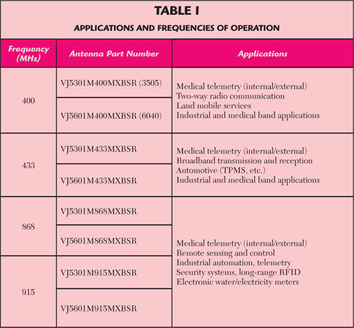
This dielectric has opened the path for further miniaturization of chip antennas in a greater factor than is available with existing technologies. This composition can reduce the size of the antenna by a factor of 20 – a significantly larger size reduction than the 5.3 offered by LTCC materials. The formulation is RoHS compliant and allows excellent stability throughout a temperature range of -40° to +85°C. A variety of different ceramic chip sizes are possible. Table 1 contains examples for two ceramic antenna chips sizes: 3505 (35 × 5 mm) and 6040 (15 × 10 mm) with additional sizes under development (thickness is 1.2 mm).
The Tuning Circuit
The antenna tuning circuit functions as an impedance matching network that matches the antenna’s impedance for maximum power transfer. Utilizing a tuning circuit, the antenna is tuned to a fixed center frequency in the UHF band. The imaginary part of the impedance can be either positive (capacitive) or negative (inductive) inside the desired frequency band. The imaginary impedance can be negated by adding one or more passive reactive components. Once the imaginary part is negated, only the real part remains, which is adjusted to 50 Ω. Thus, the antenna is tuned to 50 Ω at the desired frequency.
It is important to note that the antenna can be tuned to any desired impedance using shunt reactive elements to manipulate both the real and imaginary impedance. Using the tuning circuit, the antenna is thus tuned at a given point, thereby creating a relatively narrow band antenna, or a single-frequency antenna.
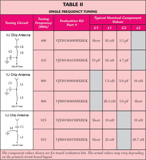
Examples of matching tuning circuits for given ceramic chips are provided in Table 2. Different capacitance and inductance values, in addition to circuit layout, can be applied based on the specific application. The table also lists the tuning element for a given frequency and chip antenna size.
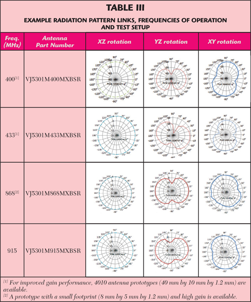
Examples of Radiation Patterns
As explained, the antenna system is constructed of a ceramic chip and a tuning circuit. Their assembly results in a platform that allows evaluating the antenna performance at the single frequency. This assembled configuration is referred to as an antenna evaluation kit (EVK). The ceramic chip antenna radiation patterns for Vishay’s EVKs are shown in Table 3.
To provide design engineers with the recommended circuit design layout, and to demonstrate the performance of the chip antenna, EVKs are used. The EVK contains a chip antenna mounted on a 40 × 90 mm printed circuit board (PCB), with a 3.5 mm SMA launch connector for transmission or reception of signals. The SMA connector allows for easy connection to the designer’s circuitry. Figure 1 demonstrates a peak gain of 1 dBi realized with 50 Ω impedance matching. The EVK also allows for the testing of the open field radiation emission. Open field radiation emission testing for this chip antenna demonstrates it has omni-directional radiation patterns.
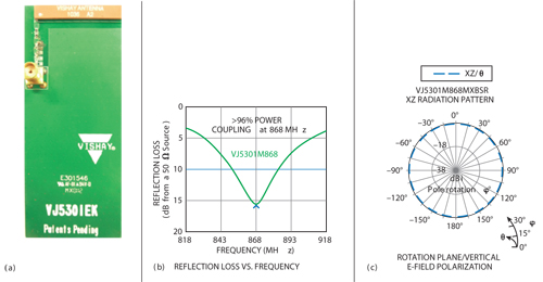
Figure 1 Example EVK (a), S11 reflection loss (b) and radiation pattern of chip antenna (c).
Miniature tunable surface-mount ceramic chip antennas that cover the UHF frequency band from 400 to 915 MHz are available. The chip antennas can be used in industrial, scientific, and medical short-range device (ISM/SRD) radio bands for applications such as medical biotelemetry receivers (400 to 433 MHz), industrial RFID applications (868 to 915 MHz), wireless security systems, sensors and remote controls. With properly selected discrete L-C tuning components, all Vishay antennas can be tuned to any regional frequency in the 400 MHz to 1.1 GHz band.
These low-profile ceramic antennas are available in small case sizes, which makes them good solutions when instrument size and/or PCB area are limited, such as in RFID sensors, garage door openers, remote controls, wireless microphones, headphones, and more. The chip antennas are mounted onto PCBs using standard surface-mount assembly methods. Single-frequency tuning is easily achieved with just a few discrete capacitor and inductor components.
Vishay Intertechnology,
Malvern, PA,
chipantenna@vishay.com,
www.vishay.com