
A non‑uniform drain line distributed power amplifier (DPA) employing a broadband impedance transformer is presented. The DPA is based on GaAs PHEMT technology. The impedance transformer employs asymmetric coupled lines and transforms a low output impedance of the amplifier to a standard 50 Ω transmission line. The output power of approximately 600 mW, with an associated gain of 9 dB and PAE greater than 30 percent, is demonstrated in the frequency range from 10 to 1800 MHz.
Distributed power amplifiers (DPA) are known for their flat gain, linear phase response and low return losses over a wide bandwidth.1 The power-added efficiency (PAE) of the conventional DPA, however, does not typically exceed 20 percent. The degradation is primarily caused by the fact that the drain current is split into two branches forming waves traveling toward the output load and the dummy termination. Several research groups have addressed the problem of DPAs’ low efficiency and limited output power, suggesting solutions to overcome these limitations.2,3 To increase the DPA efficiency, the drain current from each transistor must be pushed toward the load termination. In this way, the effect of the drain dummy termination can be mitigated.2 Another design methodology for a non-uniform DPA, employing optimal loading for each device to maximize power and efficiency, has been demonstrated.3 K. Krishnamurthy et al4 have described a DPA without an output synthesized transmission line, where delay equalization is provided by impedance-matching sections between common-source and common-gate devices.
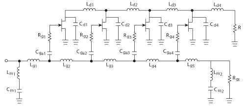
Figure 1 Simplified four-section DPA adopting a non-uniform drain line.
This article discusses an alternative design approach, based on virtual impedance analysis, considering multi-current sources and adopting a coupled line impedance transformer. The described approach leads to an increase in efficiency up to the levels required by software defined radio (SDR) driver PA applications.
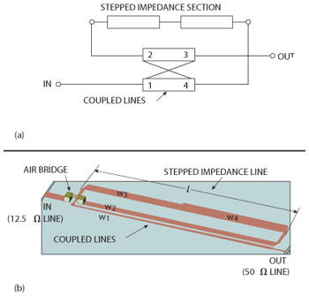
Figure 2 Compact impedance transformer (a) circuit diagram and (b) microstrip realization.
Design Approach
In the DPA topology shown in Figure 1, each device contributes to the overall output impedance of the amplifier. The value of the load impedance R is chosen for optimal power performance across the required frequency range of the four-section PHEMT DPA with non‑uniform drain line. An m‑derived section is implemented at both terminations of the gate line. Each device is supplied with 5 V, while a bias voltage of 0.44 V is applied to each gate, resulting in Class AB operation for the active devices. The necessary phase velocities synchronization between the gate and drain lines is achieved by adopting a non-uniform gate line design and selecting an output load R equal to 12.5 Ω.
In order to match the entire circuit to a standard 50 Ω load over the broad frequency range of operation, a wideband impedance transformer having a transformation ratio of 1:4 has been implemented. The impedance transformer employed in this design is based on asymmetric, uniform coupled lines as shown in Figure 2, where the dimensions are l = 42.14 mm, w1 = 0.53 mm, w2 = 1.57 mm, w3 = 1.21 mm and w4 = 1.5 mm. Coupled transmission lines have the advantage of greater flexibility and compactness, as compared to traditional multiple quarter-wavelength transmission lines.5 Traditionally, coupled and through ports of the coupled lines are either short- or open-circuited, which is not the optimal choice from a bandwidth point of view. When loading the coupled and through ports with a stepped impedance transmission line, the operating bandwidth of the transformer can be considerably increased. The adopted configuration in this case is a quarter-wavelength long and provides a three times wider operating frequency range, compared to the traditional quarter-wave transformer.
The performance of the broadband impedance transformer was verified with a full-wave 3D simulator. The input, (port 1) is terminated with a 12.5 Ω line and port 3 is connected to a 50 Ω SMA connector. Since port 1 will be connected to a 50 Ω SMA connector in real measurement, the two-port S-parameter data of the connector must be de‑embedded for accurate results. The measured insertion loss results in less than 1.5 dB across the operating bandwidth.
A medium power PHEMT device (ATF511P8 from Avago Inc.) is selected for amplifier realization. The drain loading effect of this device is negligible, however the reactive part of its output impedance (Xopt(ω)) plays an important role in defining the drain line cut‑off frequency fc. The value of the output capacitance Copt is extracted (including parasitics of the package), resulting in 4 pF. The cut-off frequency of the amplifier then can be estimated by
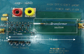
Figure 3 Photograph of the high-efficiency DPA prototype board.
Therefore, to achieve an fc of approximately 2 GHz, the values for the drain inductances Ldi (here i = 1…4) can be selected.6 The dummy drain termination is omitted, improving the overall efficiency.6
Measurement Results
In order to experimentally validate the concept of high efficiency DPA with broadband impedance transformer, a prototype circuit has been fabricated using Rogers’ three‑layer printed circuit board (PCB) material, with a relative permittivity εr = 3.66 and a thickness h = 0.762 mm. A series gate resistor Rg(k) = 5 Ω is used at each section for stability purposes. The top layer is used for lumped components as well as RF and DC line routing. A photograph of the fabricated DPA board is shown in
Figure 3. The effective size of the DPA is 24 × 74 mm.
The measured large signal DPA characteristics are shown in Figure 4. An output power of ~600 mW, a gain of 9 dB and a PAE exceeding 30 percent are achieved. A good agreement between simulation and measured results is obtained. This proves that the PAE is greater than 38 percent at low frequencies. An efficiency of more than 30 percent is recorded across the bandwidth of operation. It is evident from the measurement results that the concept to achieve high efficiency is demonstrated. Nevertheless, the DPA performance at higher frequency operation can be improved further with transformer optimization.
A transformer concept9 is an alternative solution to be integrated with the proposed DPA. On the other hand, a high power performance covering from 100 to 1800 MHz was demonstrated, using GaN HEMT,7,8 which is suitable for high output power level of SDR applications.
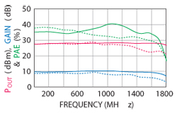
Figure 4 Measured (dotted line) and simulated (solid line) results of the DPA as a function of frequency.
Conclusion
A DPA employing a non‑uniform drain line is presented in this article. The chosen architecture exhibits improved characteristics in comparison to the traditional designs in terms of efficiency. The efficiency and output power of the amplifier is further improved by decreasing the value of the output impedance. The output impedance of the amplifier is then transformed to the standard 50 Ω termination, using a compact and broadband distributed impedance transformer based on coupled transmission lines. The proposed approach allowed increasing the efficiency of the DPA to typically better than 30 percent over a wide frequency range. The resulting circuit exhibits a power performance suitable for SDR DPA driver applications.
References
- J.B. Beyer, S.N. Prasad, R.C. Becker, J.E. Norman and G.K. Hohenwarter, “MESFET Distributed Amplifier Design Guidelines,” IEEE Transactions on Microwave Theory and Techniques, Vol. 32, No. 3, March 1984, pp. 268-275.
- L. Zhao, A. Pavio, B. Stengel and B. Thompson, “A 6 Watt LDMOS Broadband High Efficiency Distributed Power Amplifier Fabricated Using LTCC Technology,” 2002 IEEE MTT-S International Microwave Symposium Digest, pp. 897-900.
- C. Duperrier, M. Campovecchio, L. Roussel, M. Lajugie and R. Quere, “New Design Method of Uniform and Nonuniform Distributed Power Amplifiers,” IEEE Transactions on Microwave Theory and Techniques, Vol. 49, No. 12, December 2001, pp. 2494-2499.
- K. Krishnamurthy, S.I. Long and M.J.W. Rodwell, “Cascode Delay Matched Distributed Amplifiers for Efficient Microwave Power Amplification,” 1999 IEEE MTT-S International Microwave Symposium Digest, pp. 819-821.
- T. Jensen, V. Zhurbenko, V. Krozer and P. Meincke, “Coupled Transmission Line as Impedance Transformer,” IEEE Transactions on Microwave Theory and Techniques, Vol. 55, No. 12, December 2007, pp. 2957-2965.
- K. Narendra, L. Anand, M.F. Ain, S. Pragash, S. Assan and V. Zhurbenko, “High Efficiency 600 mW pHEMT Distributed Power Amplifier Employing Drain Impedance Tapering Technique,” 2008 IEEE International Conference on Microwave and Millimeter Wave Technology Digest, pp. 1769-1772.
- K. Narendra, E. Limiti, C. Paoloni, J.M. Collantes, R.H. Jansen and S. Yarman, “Vectorially Combined Distributed Power Amplifier for SDR Applications,” IEEE Transactions on Microwave Theory and Techniques, Vol. 60, No. 10, October 2012, pp. 3189-3200.
- K. Narendra, E. Limiti, C. Paoloni, J.M. Collantes, R.H. Jansen and B.S. Yarman, “Vectorially Combined Distributed Power Amplifier with Load Pull Determination,” Electronics Letters, Vol. 46, No. 16, August 2010, pp. 1137-1138.
- V. Zhurbenkho, K. Sim and K. Narendra, “A Compact Broadband Nonsynchronous Noncommensurate Impedance Transformer,” Microwave and Optical Technology Letters, Vol. 54, No. 8, August 2012, pp. 1832-1835