
Today’s transmitters for earth imaging micro-satellite systems demand higher communication quality and higher data rates to be capable of transmitting pictures or data with an appropriate quality, a higher frequency of operation and more channels per unit bandwidth. Low power consumption and small size are also required for this equipment. All of these constraints combine to make the whole design, including component selection and evaluation, quite challenging. One portion of this design that is very critical with regard to all of the requirements mentioned above is the synthesized oscillator.1 This article describes the design of an X-band frequency synthesizer that can be used in micro-satellite transmitters. It discusses the design of the phase-locked loop (PLL) and the phase noise in each component of the circuit (voltage-controlled oscillator (VCO), phase detector, temperature-compensated crystal oscillator (TCXO), dividers and loop filter). In the simulation, the reference spurs and their effect on the noise performance of the PLL frequency synthesizer are also included. The accuracy of the values calculated for the loop filter is crucial to the success of this design. In the present case, the loop filter is accurately evaluated by using an efficient estimation technique.
An X-band VCO requires a low noise, high frequency prescaler to bring its output frequency into the range of the existing PLL for phase locking. Frequency multipliers and dividers are now available to simplify the design and implementation of X- and Ku-band synthesizers. In the simulation, the characteristics of commercially available components are considered. The high stability crystal reference oscillator is a 10 MHz TCXO from Voltronics; the phase-locked loop is a National Semiconductor 2326 component, capable of phase locking a VCO between 500 MHz and 3 GHz. For this reason, a Hittite (12 GHz, 1/8) prescaler was used to extend the frequency into X-band.

Design and Theory
Figure 1 shows the PLL’s linear model with feedback. This PLL is called an integer-N system, which means that the VCO frequency and the crystal reference are some integer multiple of the reference frequency. The PLL consists of a high stability crystal reference oscillator, a frequency synthesizer, a voltage-controlled oscillator and a passive loop filter. The frequency synthesizer includes a phase detector, a current mode charge pump and programmable frequency dividers. The passive filter is desirable for its simplicity, low cost and low phase noise. If the input signal to the PLL is
![]()
and the output signal for the VCO is assumed to be

Assuming that ωy = ωr, the output from the phase detector is expressed as

where
θr = input phase
θy = output phase
θe = phase error
Kp = phase-detector/charge-pump gain factor
The VCO is assumed to be a linear device whose output frequency varies proportionally to the loop filter voltage Vf(t), and is expressed by
![]()
where
f0 = free-running frequency
KVCO = VCO’s gain factor or tuning coefficient expressed in MHz/V
Since the phase is the integral of the angular velocity, the VCO is modeled as
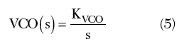

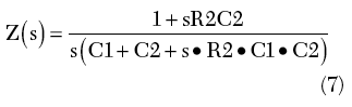
Figure 2 shows the third-order low pass filter introduced in this model by its transfer function F(s) described by Equation 6 and applicable to this system, which requires a third pole for additional reference suppression

where Z(s) describes the transfer function of the second order loop filter given by
Combining these transfer functions gives the open loop gain

To achieve optimal circuit performance, the phase noise should be evaluated for proper loop design. It will impact many critical operating characteristics of the synthesized oscillator, including adjacent channel power. Phase noise in a PLL can originate from a number of sources. The well-known noise sources are specifically the crystal reference (TCXO) noise, the phase detector noise and the VCO phase noise. If a TCXO is used, its phase noise data should be obtained from the manufacturer so that the reference values can be used in the model. A simple approximation for this noise source due to the crystal reference itself, as with any oscillator, is that it is inversely proportional to the offset frequency.2 Higher order approximations are required for more accuracy, but the 1/f approximation is a good starting point for this study.
The VCO noise can be modeled as a simple approximation inversely proportional to the offset frequency from the carrier. The noise of the VCO is effectively high pass filtered by the PLL, providing rejection of phase noise or phase error within the bandwidth, but leaving the VCO noise well outside of the loop bandwidth unaffected. The VCO noise is given by3
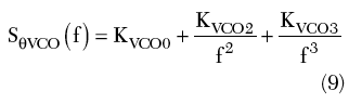

where the three coefficients in the VCO noise equation were determined to yield the specific noise at the particular offsets from the carrier.
The phase detector noise represents the internal noise floor of the phase/frequency detector and frequency dividers within the PLL. For the National Semiconductor synthesizer used in this work, the phase detector noise floor is given for an effective reference frequency of 1 Hz. This noise is shaped by the closed loop transfer function G(f) of the synthesizer as4

It is well known that the reference sidebands and spurious outputs play a major role in determining the noise properties of a PLL frequency synthesizer. Reference spurs are unwanted noise sidebands that can occur at multiples of the comparison frequency, and can be translated in the transmitter subsystem by the mixer to the desired signal frequency. The power of the reference spur is expressed by2


where Fspur will be assumed to be a multiple of the comparison frequency.
Aside from spur gain, the spur’s noise is also caused by mismatches and leakages in the charge pump of the PLL. These two factors in the charge pump can cause an AC modulation on the tuning line of the VCO, which can be viewed as FM modulation. This FM modulation gives rise to reference spurs. The spur level is given by2

where the leakage spur is the dominant term of the reference spurs caused by the leakage effects at lower comparison frequencies. However, the mismatch is the dominant factor at high comparison frequencies.
Results and Discussions
For the design described in this article, a Matlab program was used to simulate the circuit. In the simulation, the characteristics of a National Semiconductor model LMX2326 programmable frequency synthesizer and a VCO with a 50 V/MHz sensitivity were used. The VCO is from General Microwave, which utilizes a high performance transistor operating at the fundamental, rather than the doubling push-push mode. A commercial 10 MHz temperature-compensated crystal oscillator from Voltronics with a specified noise of approximately –110 dB/Hz at an offset frequency of 10 kHz is used. The PLL using the LMX2326 component is capable of phase locking a VCO between 500 MHz and 3 GHz. For this reason, to extend the frequency range in the X-band frequencies, a (12 GHz, 1/8) prescaler from Hittite was used. The HMC363 prescaler is a low noise divide-by-8 static divider using an InGaP/GaAs heterojunction bipolar transistor (HBT) technology and has a phase noise of –153 dBc/Hz at an offset frequency of 100 kHz, which helps the user maintain good system noise performance. In practice, the PLL can be programmed via a laptop computer and parallel port cable. The frequency changes were done using software provided by National Semiconductor, in which the PLL serial-control data are controlled by three inputs (data, LE and clock). For regulating the channel frequency, the serial data input is designed to control the 15 b of the R counter and 18 b of the N counter (which includes 7 b from the A counter and 11 b from the B counter). In this example, a frequency range of 8025 to 8175 MHz and a channel spacing of 1 MHz are required. So, for the reference divider (R counter) equal to 10 (00000000001010)b and the N counter equal to 1010 : (A counter = 18 (0010010) and B counter = 31 (00000011111)), the output frequency resulting (P1 ¥ (32 ¥ B + A) ¥ reference frequency) is equal to 8080 MHz.

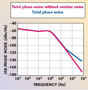
Figure 3 shows the total phase noise with and without the resistor noise sources. Note that the reference spurs are not included in the total phase noise. The results show that within the loop bandwidth (10 Hz to 10 kHz) of the synthesizer, the level of the reference oscillator is higher because the closed loop transfer function is very large in magnitude and it drops off rapidly when it reaches the loop bandwidth. The results also show that the resistor noise contribution is very small at the synthesizer output. The R2 and R3 noise versus frequency is shown in Figure 4. To demonstrate that the noise of the VCO is high pass filtered by the PLL, providing rejection of the phase noise or phase error within the bandwidth, Figure 5 shows the loop error response, which is obtained by the connection between the open and closed loop responses.
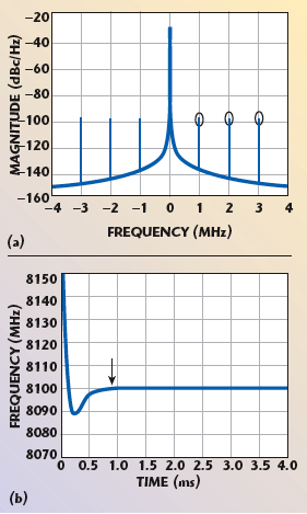
In this approach, the loop filter design is a very critical part of the PLL synthesizer. In general, a low loop filter cut-off frequency does not suppress the phase noise at close-in frequencies because the closed loop negative feedback region is narrowed. In addition, it makes the PLL response slower and the settling time of the frequency switching (PLL lockup time) longer and, as a result, the PLL spurious is suppressed. Conversely, increasing the cut-off frequency provides a faster PLL response and a shorter PLL lockup time. However, the PLL output signal is frequency-modulated and contains high level spurs. Since the sideband’s spurious noise affects the adjacent channels, the unwanted spurs can be suppressed by narrowing the loop filter bandwidth.5 An accurate estimation of the loop filter is used, which guarantees the precision of the design. The output spectrum and the transient response plots for two low loop filters with different cut-off frequencies are shown in Figures 6 and 7, where the spurious level, phase noise and frequency transient are evaluated under various conditions.
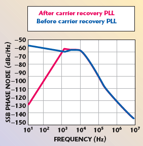
Figure 8 shows the effect of the carrier recovery PLL in demodulation on the level of the single-sideband (SSB) phase noise and demonstrates the phase noise rejection properties of the carrier recovery PLL. The carrier recovery PLL suppresses the 100° deviation at 100 Hz down to a level that eliminates crossings of the decision boundaries. Integration of this curve on both sides of the carrier results in an rms phase noise of 0.008 radians, and a margin of signal-to-noise ratio (S/N) of 22.36 dB.
Conclusion
A simple design of an X-band frequency synthesizer that can be applied to micro-satellite transmitter systems has been presented. This article has discussed the phase noise from different sources in the PLL and their effects on the noise performance of the system and has demonstrated that the loop filter cut-off frequency choice is very important to achieve the performed PLL’s spurious level, phase noise and frequency transient. To guarantee the precision of the design, an accurate estimation of the loop filter was used. The results indicate that for a frequency range of 8025 to 8175 MHz and with a carrier recovery of 0.6 kHz, the PLL gives an rms of 0.008 radians and a signal-to-noise ratio of 22.36 dB.
References
1. A. Hajimiri and T. Lee, “A General Theory of Phase Noise in Electrical Oscillators,” IEEE Journal of Solid State Circuits, Vol. 33, No. 2, February 1998, pp. 179–194.
2. D. Banarjee, PLL Performance, Simulation and Design, Second Edition, National Semiconductor, 2001.
3. E. Drucker, “Model PLL Dynamics and Phase-noise Performance,” Microwaves & RF, Vol. 35, No. 2, February 2000, pp. 73–82.

Mohamed Kameche
4. L. Lascari, “Accurate Phase Noise Prediction in PLL Synthesizers,” Applied Microwave and Wireless, Vol. 12, No. 2, February 2000, pp. 30–38.
5. M. Kameche and L. Hadj Abderahmane, “Design an X-band Frequency Synthesizer for Small Satellites,” CD Proceedings of the 9th International Space University Annual International Symposium: “Civil, Commercial and Security Space: What Will Drive the Next Decade?,” Strasbourg, France, November 30–December 3, 2004.
Mohamed Kameche received his diploma in electrical engineering and his master’s degree in signal and systems from the University of Tlemcen, Algeria, in 1998 and 2001, respectively. From 1998 to 2001, he was a teaching member in the department of electronics at the University of Tlemcen. He is currently with the National Center of Space Techniques (CNTS) at Arzew, Oran, Algeria. His research interests include temperature effects on RF and microwave devices and package modeling for microwave circuit applications.