
With the increasing demand for smartphones and tablets in the world and the growing need for high data rates, wireless semiconductor manufacturers are exposed to the convergence of multiple market and technology forces, pressing them to look for new architectures and technology innovations in their RF components test environments.
- The fragmentation of frequency ranges, combined with the increasing number of modulation schemes and RF paths, creates an exponential growth of test scenarios. Up to 1 million tests may be required during the characterization phase of latest generation RF components.
- Component test time needs to be reduced to minimize supply response time, match market windows and keep competitive price points.
- Wider bandwidths, such as 160 MHz for the new WLAN 802.11ac standard, are driven by the need for higher data rates. These new standards are expanding the test stations requirements and challenging calibration techniques.
One of the key instruments in a wireless test station is the Vector Signal Generator (VSG). This equipment will generate either ideal or complex real world signals to test the performance of RF components under a large number of test scenarios. To increase the test speed, the VSG must quickly change stimulus parameters, such as signal frequency, power and waveforms. VSG architectures have been improved over the years, but the traditional analog frequency and amplitude tuning speeds are optimized to a point where any speed increase may be achieved at the expense of signal quality.
An innovative tuning technique, enabled by digital baseband processing technology, helps break the speed barrier without compromise on the signal quality within latest generation VSGs. This article discusses the typical limitations of RF tuning, the theory behind digital baseband tuning, its advantages and how it can be used to accelerate RF component test.
Device Types and Test Speed Requirements
Production and pre-production testing are the most demanding environments for high speed testing. When thinking about mobile devices, there are three major testing periods in the production food chain: assembled mobile device, RF boards and RF components.
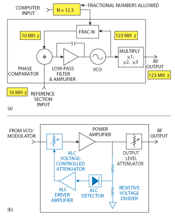
Figure 1 Traditional VSG architectures utilize two important loops to ensure accurate frequency (a) and amplitude (b) levels.
During production testing of the assembled mobile device, the speed of the test process is often limited by the mobile device itself. Test response time for a mobile device is typically measured in milliseconds.
At the board level, testing is performed at all frequencies and power levels. Due to the huge number of tests, the key components are set into a special test mode which sequences through the entire test with a 5 ms step (typical) between data collection points. For the VSG, it must be able to stay in step with this sequence rate. Latest generation VSGs, when used in list mode, have analog RF tuning speed around 220 µs and can stay synchronized with the DUT’s test sequence.
The ultimate speed challenge occurs at the component level of the wireless food chain. There are several key RF components that require performance testing of each device: power amplifiers, transceivers, front-end modules (FEM), and often a system on chip (SoC) for WLAN/Bluetooth/RF tuner. Testing these components will require the test instrumentation and VSG to work at the highest possible speed.
One example of a time consuming test sequence is the power loop test scenario. Performance measurements of a power amplifier or front-end module are normally made at a specific output level of the DUT. Since all devices have variations in gain, it is necessary to run multiple iterations of the input power level to reach the desired output level. Getting the loop to quickly converge requires very high switching speed and excellent linearity and repeatability of the VSG. Only after the DUT output level is set at the correct value can the specified parameters be tested. Reducing the number of iterations while accelerating the switching time between each iteration has a significant impact on the test speed.
Maximizing Analog RF Tuning Speeds
Latest generation PXI VSGs offer analog RF tuning at speeds as fast as 220 µs in list mode for both amplitude and frequency changes. There are two important mechanisms that limit speed within a VSG: the frequency synthesizer and the amplitude leveling control (see Figure 1).
The frequency synthesizer has an output frequency whose accuracy is directly related to the 10 MHz reference. The phase-lock-loop that compares these two signals and optimizes the phase noise typically has a settling time of a millisecond. Over the years, a number of proprietary techniques have been established to minimize the PLL settling time for frequency changes and reach hundreds of microseconds frequency switching time.
A VSG includes many active components that are temperature sensitive. The amplitude leveling control (ALC) is a real-time loop that monitors the output level and maintains a constant output level. There are a number of techniques to optimize the ALC settling time after changing amplitude or frequency. In addition, a full featured VSG will typically offer multiple modes including ALC On, ALC Off and ALC hold modes so the ALC can be turned off to achieve the fastest speeds. A typical optimized source can settle within 0.2 dB in about 500 µs.
Optimizing tuning speeds and signal quality is where test equipment vendors have invested a lot of IP over the years. An architectural advancement was needed to dramatically improve the VSG’s measurement speed without compromising the signal quality required by today’s wireless standards.
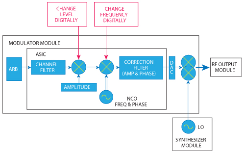
Figure 2 Digital baseband tuning changes the frequency and amplitude level digitally within the specified bandwidth of the VSG.
Introducing Digital Baseband Tuning
Digital baseband tuning techniques offer the ability to digitally shift both the frequency and amplitude levels of the signal within the VSG’s available modulation bandwidth without the need to retune the synthesizer (see Figure 2). As new generation VSGs offer larger modulation Bandwidths, the digital baseband allows wider frequency shifts.
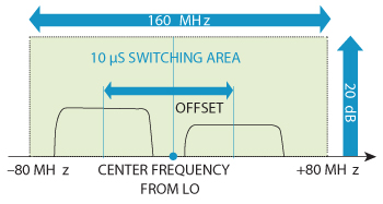
Figure 3 Within a 160 MHz bandwidth range, simultaneous frequency shifts and amplitude level changes can be made in 10 µs over a 20 dB range.
The maximum frequency shift is dependent on the modulation bandwidth of the VSG. For example, within a 160 MHz bandwidth, this technique enables frequency shifts to be achieved in 10 µs, an order of magnitude faster than analog tuning techniques. The same speed also applies to any level change within typically a 20 dB range. Of course the actual signal bandwidth has to be considered within this tuning range. For example, a 5 MHz WCDMA signal can have a 155 MHz of frequency offset range. An 80 MHz 802.11ac signal can only be offset ±40 MHz. To take advantage of the 10 µs switching speeds, test plans should perform all tests within the VSG’s bandwidth range first, prior to taking larger frequency or amplitude steps. These larger steps outside of the VSG’s bandwidth require 220 µs. Then a new VSG bandwidth tuning window is available with 10 µs switching (see Figure 3).
These extremely fast performance improvements are enabled by proprietary ASICs. The ASIC includes several important processing functions inside the VSG’s modulator module including:
- Real-time numerical controller oscillator for frequency offset
- Real-time multiplier for amplitude offset
- Real-time signal correction, based on fully characterized RF and IF path
How the Frequency and Amplitude Level are Changed Digitally
For frequency changes that occur within the baseband tuning bandwidth, let’s examine what is occurring inside the processing chain that enables the digital frequency shift. Assume that a sampled complex waveform, s(nT), is stored in memory on the VSG. It will be processed, sent to the DACs, and then upconverted to the desired center frequency by the IQ modulator.
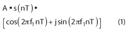
In the time domain, the sampled waveform is multiplied by the numerically controlled oscillator’s (NCO) complex sinusoid:
The scaling factor, A, allows the amplitude level to be adjusted.
Multiplication by a complex sinusoid in time domain is equivalent to convolution in the frequency domain with the impulse function δ(f):

This results in a frequency shift of the original signal’s spectrum:
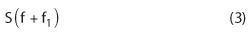
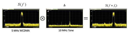
Figure 4 The input waveform S(f) is convoluted with the digitally created shift frequency, S(f1), to produce very fast, accurate frequency and level changes, S(f + f1).
Figure 4 shows an example of this process using a 5 MHz wide WCDMA waveform which is shifted up in frequency by 10 MHz. When this process is done in the analog world, special filtering is required to eliminate unwanted sum and difference terms that are generated in the process. When frequencies are shifted in the digital world, there are no negative frequencies or other error terms generated. Therefore, the mathematical ideal frequency shift does not require any filtering. To digitally shift frequencies, all that is needed is a sine lookup table, a cosine lookup table, and a complex multiplication algorithm. This process occurs in real-time in the ASIC across the 160 MHz baseband tuning range. In Figure 4, a few low level spurs in the resulting signal may be seen. These are residual errors from the analog IQ modulator that include signal images and carrier feed through.
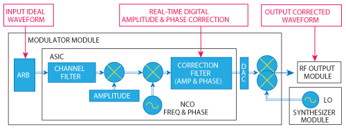
Figure 5 Test engineers input their desired waveforms and the VSG's real-time correction capability ensures both amplitude and phase linearity.
Real-Time Corrections
Narrow bandwidth VSGs (< 40 MHz) have been able to use single values for correcting quadrature and gain imbalance across the tuning bandwidth. When the tuning ranges extend to 160 MHz, a more thorough real-time correction process is required to meet the linearity needs of today’s higher data rates.
The optimal way to maintain highest signal quality is to include a correction filter using 2×2 matrix taps that offers full magnitude and phase correction across the entire 160 MHz tuning band (see Figure 5). The entire IF and RF path of each VSG must be completely characterized during manufacturing calibration, and the resulting complex data are stored in the modulator and RF output module’s flash memory. This data is used during runtime to construct and load a new 160 MHz wide complex correction filter whenever the RF center frequency or RF attenuator state changes. This provides exceptional magnitude and phase corrections up to the RF output (see Figures 6 and 7).
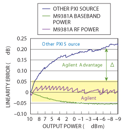
Figure 6 Digital baseband tuning enables accurate linearity across a 20 dB leveling range. The speed improvement of 10 µs vs. 250 µs for RF power leveling offer only a very small degradation in linearity.
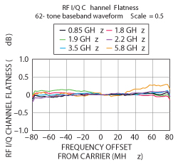
Figure 7 Wider tuning bandwidths require full matrix real-time corrections to achieve accurate linearity.
To take advantage of digital baseband tuning for power amplifier testing, engineers can set the RF frequency to the center of the band being tested and the RF power level to the maximum required for all tests. From there, baseband frequency adjustments are made to test at multiple frequencies across the band and the baseband power level is adjusted servoing the DUT output level to the correct value. Better linearity, repeatability and resolution further reduce the test time by enabling the servo loop to converge in fewer steps. Figure 6 shows the measured linearity of the M9381A over a 20 dB range from +10 to –10 dBm, using both the baseband and RF level adjustments.
Conclusion
With billions of components going into mobile wireless devices, reducing test times can have a major cost benefit. As device data rates continue to increase, reducing test times while maintaining signal quality adds new test station challenges.
Digital baseband tuning introduces a new VSG architecture that is dramatically faster than traditional RF tuning techniques. Signal quality is maintained due to new real-time matrix correction techniques that are applied across the entire 160 MHz tuning bandwidth. This results in excellent amplitude and phase linearity to assure the signal quality required by increasingly demanding wireless standards.