
One of the most important parameters for oscillators is phase noise as it is critical to most applications.1-21 There are several methods for measuring phase noise which will be covered here including the pros and cons of each technique. Example measurements on various types of systems will also be compared including their accuracy and speed.
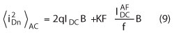
The pioneer in phase noise measurement was Hewlett Packard.1,2 Modern phase noise systems use the correlation principle but this method has some drawbacks. The most direct and sensitive method to measure the spectral density of phase noise, SΔθ(fm), requires two sources – one or both of them may be the device(s) under test – and a double balanced mixer used as a phase detector (see Figure 1). The RF and LO input to the mixer should be in phase quadrature, indicated by 0 V dc at the IF port. Good quadrature assures maximum phase sensitivity Kθ and minimum AM sensitivity. With a linear mixer, Kθ equals the peak voltage of the sinusoidal beat signal produced when both sources are frequency offset.
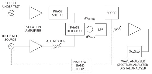
Figure 1 Phase noise system with two sources maintaining phase quadrature.
When both signals are set in quadrature, the voltage ΔV at the IF port is proportional to the fluctuating phase difference between the two signals.
where Kθ = phase detector constant,
= V B peak for a sinusoidal beat signal.
The calibration of the wave analyzer or spectrum analyzer can be read from the equations. For a plot of L(fm), the 0 dB reference level is to be set 6 dB above the level of the beat signal. The -6 dB offset has to be corrected by +1.0 dB for a wave analyzer and by +2.5 dB for a spectrum analyzer with log amplifier and average detector. In addition, noise bandwidth corrections may have to be applied.
Since the phase noise of both sources is measured in this system, the phase noise performance of one of them needs to be known in order to measure the other source. Frequently, it is sufficient to know that the actual phase noise of the dominant source cannot deviate from the measured data by more than 3 dB. If three unknown sources are available, three measurements with three different source combinations yield sufficient data to accurately calculate each individual oscillator’s performance.
Figure 1 indicates a narrowband phase-locked loop that maintains phase quadrature for sources that are not sufficiently phase stable over the period of the measurement. The two isolation amplifiers should prevent injection locking of the sources. Residual phase noise measurements test one or two devices, such as amplifiers, dividers or synthesizers, driven by one common source. Since this source is not free of phase noise, it is important to know the degree of cancellation as a function of Fourier frequency.
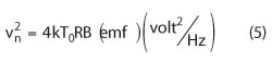
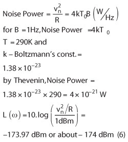
The noise floor of the system is established by the equivalent noise voltage, ΔVn, at the mixer output. It represents mixer noise as well as the equivalent noise voltage of the following amplifier:
Noise floors close to -180 dBc can be achieved with a high-level mixer and a low-noise port amplifier. The noise floor increases with fm-1 due to the flicker characteristic of ΔVn. System noise floors of -166 dBc at 1 kHz have been realized. This is the limitation of this approach.
In measuring low-phase-noise sources, a number of potential problems have to be understood to avoid erroneous data:
- If two sources are phase locked to maintain phase quadrature, it has to be ensured that the lock bandwidth is significantly lower than the lowest Fourier frequency of interest.
- Even with no apparent phase feedback, two sources can be phase locking (injection locked), resulting in suppressed close-in phase noise.
- AM noise of the RF signal can come through if the quadrature setting is not maintained sufficiently.
- Deviation from the quadrature setting will also lower the effective phase detector constant.
- Nonlinear operation of the mixer results in a calibration error and will add noise.
- A non-sinusoidal RF signal causes Kθ to deviate from VB peak.
- The amplifier or spectrum analyzer input can be saturated during calibration or by high spurious signals such as line frequency multiples.
- Closely spaced spurious signals such as multiples of 60 Hz may give the appearance of continuous phase noise when insufficient resolution and averaging are used on the spectrum analyzer.
- Impedance interfaces should remain unchanged when going from calibration to measurement.
- In residual measurement system phase, the noise of the common source might be insufficiently canceled due to improperly high delay-time differences between the two branches.
- Noise from power supplies for devices under test or the narrowband phase-locked loop can be a dominant contributor of phase noise.
- Peripheral instrumentation such as the oscilloscope, analyzer, counter or DVM can inject noise.
- Microphonic noise might excite significant phase noise in devices.
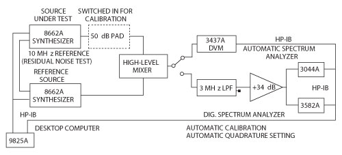
Figure 2 Automatic system to measure residual phase noise of two 8662A synthesizers (courtesy of Hewlett-Packard Co.).
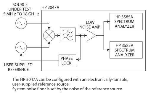
Figure 3 Block diagram of HP 3047A.
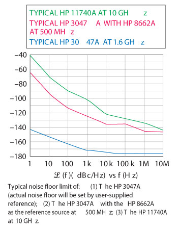
Figure 4 Typical noise floor limit.
Despite all these hazards, automatic test systems have been developed and operated successfully for years.4 Figure 2 shows a system that automatically measures the residual phase noise of the 8662A synthesizer. It is a residual test, since both instruments use one common 100 MHz referenced oscillator. Quadrature setting is conveniently controlled by probing the beat signal with a digital voltmeter and stopping the phase advance of one synthesizer when the beat signal voltage is sufficiently close to zero.
Doing Measurements
As shown in Figure 3, the Hewlett Packard test equipment HP3047A was built around a double-balanced mixer which can handle +23 dBm of power. While this HP equipment is no longer manufactured and has been replaced by the Agilent E5052A and E5052B, this system shows some interesting features.
- The noise floor is about −177 dBc/Hz and the resolution, shown in Figure 4 is approximately −180 dBc/Hz.
- The limit of the dynamic range is (Pout (dBm) + kT – NF), (where NF = NFosc + NFamp) which in the case of a 0 dBm oscillator would be −174 dBc or relative to one sideband −177 dBc - NF. Assuming a signal to be +20 dBm, then the dynamic range is approximately 200 dBc - NF.
- The term NFosc refers to the large signal noise figure of the oscillator, which can vary from 2 dB at 10 MHz to 6 dB at 100 MHz or even higher at 1000 MHz. As an example, the far out SSB noise at 1000 MHz is typically −172 dBc/Hz at 5 dBm of output power.
- The mixer and the post amplifier can easily go into compression which raises the noise floor. In the previous publications for this system, this effect was not considered. It was found that some of the measurements done with this system at low frequencies were off, the crystal oscillators in question were actually better.
From a system’s point-of-view, the numbers are not that optimistic, as seen from Figure 5. The reason for this is that the transistor used in the oscillator has its own noise contribution. This system is used to measure residual noise in amplifiers or switches. This is an important diagram for system planning.
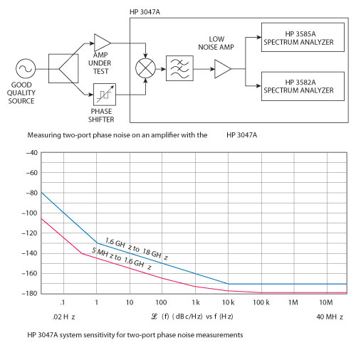
Figure 5 The HP 3047A residual phase noise measurement, not oscillator phase noise.
The HP 3047A has a built-in crystal oscillator and its measured phase-noise is shown in Figure 6. These measurements are actually a little better than what was specified by HP but these are not as good as modern measurement systems.
Synergy kept the old HP system hardware for these references. The system is software based and used an FFT analyzer; for its time this was the best system around, but the measurements took a long time to make. Modern test equipment using the cross-correlation methods are at least 20 times faster.
Noise in Circuits and Semiconductors
Figure 6 HP10811B measurement of 10 MHz signal on R&S FSUP.
Microwave applications generally use bipolar transistors and following are their noise contributions.3,5,6,9,21
Johnson Noise
- The Johnson noise (thermal noise) is due to the movement of molecules in solid devices called Brown’s molecular movements.
It is expressed as
The power can be written as:
- In order to reduce this noise, the only option is to lower the temperature, since noise power is directly proportional to temperature.
The Johnson noise sets the theoretical noise floor.
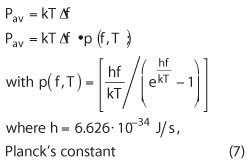
Planck’s Radiation Noise
- The available noise power does not depend on the value of resistor but it is a function of temperature T. The noise temperature can thus be used as a quantity to describe the noise behavior of a general lossy one-port network.
- For high frequencies and/or low temperature, a quantum mechanical correction factor has to be incorporated for the validation of equation. This correction term results from Planck’s radiation law, which applies to blackbody radiation.
Schottky/Shot Noise
- The Schottky noise occurs in conducting PN junctions (semiconductor devices) where electrons are freely moving. The root mean square (RMS) noise current is given by
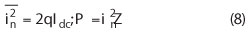
where q is the charge of the electron, P is the noise power, and Idc is the dc bias current.
Z is the termination load (can be complex).
- Since the origin of this noise generated is totally different, they are independent of each other.
Flicker Noise
- The electrical properties of surfaces or boundary layers are influenced energetically by states, which are subject to statistical fluctuations and therefore, lead to the flicker noise or 1/f noise for the current flow.
- 1/f noise is observable at low frequencies and generally decreases with increasing frequency f according to the 1/f-law until it will be covered by frequency independent mechanism, like thermal noise or shot noise.
Example: The noise for a conducting diode is bias dependent and is expressed in terms of AF and KF.
- The AF is generally in range of 1 to 3 (dimensionless quantity) and is a bias dependent curve fitting term, typically 2.
- The KF value is ranging from 1E-12 to 1E-6 and defines the flicker corner frequency.
Transit Time and Recombination Noise
- When the transit time of the carriers crossing the potential barrier is comparable to the periodic signal, some carriers diffuse back and this causes noise. This is really seen in the collector area of NPN transistor.
- The electron and hole movements are responsible for this noise. The physics for this noise has not been fully established.
Avalanche Noise
- When a reverse bias is applied to semiconductor junction, the normally small depletion region expands rapidly.
- The free holes and electrons then collide with the atoms in depletion region, thus ionizing them, and produce a spiked current called the avalanche current.
- The spectral density of avalanche noise is mostly flat. At higher frequencies, the junction capacitor with lead inductance acts as a lowpass filter.
- Zener diodes are used as voltage reference sources and the avalanche noise needs to be reduced by big bypass capacitors.
Prediction of Phase Noise
- In designing an oscillator, one needs to have a concept of how to do this and can hopefully validate the same. The basic equation (Rohde’s Modified Leeson Equation) needed to calculate the phase noise is found in The Design of Modern Microwave Oscillators for Wireless Applications: Theory and Optimization.1,13,14,15,16 It is:
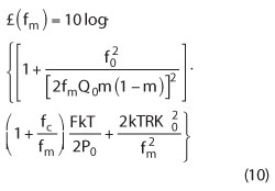
where £(fm), fm, f0, fc, QL, Q0, F, k, T, P0, R, K0 and m are the ratio of the sideband power in a 1 Hz bandwidth at fm to total power in dB, offset frequency, flicker corner frequency, loaded Q, unloaded Q, noise factor, Boltzmann’s constant, temperature in degree Kelvin, average output power, equivalent noise resistance of tuning diode, voltage gain and ratio of the loaded and unloaded Q, respectively.
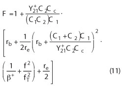
In the past this was done with the Leeson formula, which contains several estimates, those being output power, flicker corner frequency and the operating (or loaded) Q. Now, one can assume that the actual phase noise is never better than the large signal noise figure (F) given by the following equation:13,14
Applying Cross-Correlation
The old systems have an FFT analyzer for close-in calculations and are slower in speed. Modern equipment use the noise-correlation method. The reason why the cross-correlation method became popular is that most oscillators have an output between zero and 10 dBm and what is even more important is that only one source is required. The method with a delay line, in reality required a variable delay line to provide correct phase noise numbers as a function of offset (this is shown in reference 1, pp. 148-153, Fig. 7.25 and 7.26).
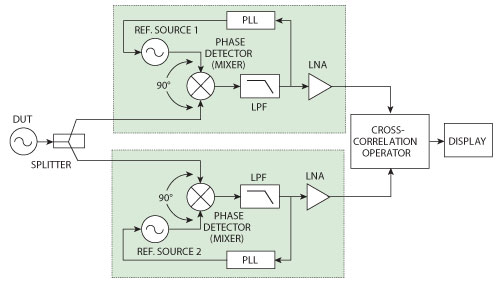
Figure 7 Block diagram showing the noise-correlation method.
This technique combines two single-channel reference source/PLL systems and performs cross-correlation operations between the outputs of each channel, as shown in Figure 7.7,8 The DUT noise through each channel is coherent and is not affected by the cross-correlation, whereas the internal noise generated by each channel is incoherent and is diminished by the cross-correlation operation at the rate of M (M being the number of correlations). This can be expressed as:
where Nmeas is the total measured noise at the display; NDUT the DUT noise; N1 and N2 the internal noise from channels 1 and 2, respectively; and M the number of correlations. The two-channel cross-correlation technique achieves superior measurement sensitivity without requiring exceptional performance of the hardware components. However, the measurement speed suffers when increasing the number of correlations.5 The built-in synthesizer limits the dynamic range and that is the reason why at lower frequencies crystal-oscillators are used.
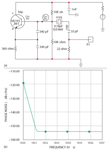
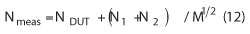
Figure 8 4 MHz low noise crystal-oscillator (U.L. Rohde, 1975) (a) and simulated phase noise (b).
The assumption is that the internal reference sources 1 and 2 are at least equal in noise contribution as the DUT and assuming a correlation of 20 dB (limited by leakage and other large signal phenomena) divider noise, those references can be 20 dB worse. Both Rohde & Schwarz and Agilent use a synthesized approach. This limits the dynamic range close-in to the carrier and far-out to the carrier. When using the correlation to get 10 dB more dynamic range, 100 correlations are necessary or the measurement is one hundred times slower. The R&S FSUP is a combination of a spectrum analyzer and the phase noise test setup while the Agilent E5052B is a dedicated system, about 4-6 times faster.
Advantages of the Noise Correlation Technique11-19
- Increased speed
- Requires less input power
- Single source set-up
- Can be extended from low frequencies like 1 MHz to 100 GHz
All of which depends upon the internal synthesizer.
Disadvantages of the Noise Correlation Technique
- Different manufacturers have different isolation, so the available dynamic range is difficult to predict.
- These systems have a “sweet-spot,” both Rohde & Schwarz and Agilent start with an attenuator, not to overload the two channels; 1 dB difference in the input level can result in significantly different measured numbers. These “sweet-spots” are different for each system. The RF attenuation that is needed to find the “sweet-spot” reduces the overall dynamic range of the correlation by this amount.
- The harmonic content of the oscillator can cause an erroneous measurement so a switchable lowpass filter (such as the R&S Switchable VHF-UHF Lowpass Filter Type PTU-BN49130 or its equivalent) should be used.6
- For frequencies below 200 MHz, systems such as AnaPico or Holzworth using two crystal oscillators instead of a synthesizer must be used (there is no synthesizer good enough for this measurement). Example: Synergy LNXO100 crystal oscillator measures about -142 dBc/Hz (100 Hz offset), limited by the synthesizer of the FSUP and -147 dBc/Hz with the Holzworth system. Agilent results are similar to the R&S FSUP, just faster.
- At frequencies like 1 MHz off the carrier, these systems gave different results. The R&S FSUP, taking advantage of the “sweet-spot,” measures -183 dBc, Agilent indicates -175 dBc/Hz and Holzworth measures -179 dBc/Hz.
We have not researched the “sweet-spots” for Agilent and Holzworth, but we have seen publications for both Agilent and Holzworth showing −190 dBc/Hz far off the carrier. These were selected crystal oscillators from either Wenzel or Pascall.
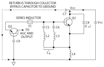
Figure 9 Rohde design later implemented by HP.
Another problem is the physical length of the crystal oscillator connection cable to the measurement system. If the length provides something like “quarter-wave-resonance,” incorrect measurements are possible. The list of disadvantages is quite long and there is a certain ambiguity concerning whether or not to trust these measurements or if they are repeatable.
Crystal Oscillators
Here are some important examples of crystal oscillators. The first one is by Rohde (1975) and is shown is Figure 8a with simulated phase noise shown in 8b.4,9 This represents the phase-noise of the oscillator without the buffer-amplifier shown inFigure 8a.Most modern equipment uses the crystal oscillator using Rohde’s design technique (see Figure 9). The actual measured numbers are shown in Figure 6. Another important oscillator is by Michael Driscoll. This circuit is shown in Figure 10a and its simulated phase noise in Figure 10b. The crystal is used as a filter to ground. We have seen applications of this design from 10 to 100 MHz. Sometimes there is a stability problem with upper transistor of the cascode. Another important contribution is the introduction of the stress-compensated or doubly-rotated crystal, in short SC cut. This took over after the AT cut. Its drawbacks are possible spurious resonance and higher cost, but the actual phase-noise is 6 to 10 dB. So far there is no clear explanation of why this is the case.10,11
Figure 10 Driscoll oscillator (a) and simulated phase noise (b).
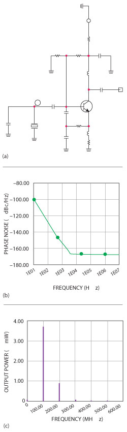
Figure 11 100 MHz crystal oscillator without buffer stage (a), simulated phase noise (b) and output power (c).
The 100 MHz crystal oscillator measurements are most demanding and these oscillators are the backbone of many test and communication equipment. Figure 11 shows a typical simple 100 MHz crystal oscillator and its simulated phase noise. Its output power is shown in Figure 11c. This oscillator is missing a buffer stage. Figure 12a shows the buffer amplifier and Figure 12b shows its simulated noise figure and Fmin. An increase in the noise figure, seen below 50 MHz, is due to coupling capacitor. Finally, a 100 MHz crystal oscillator with a grounded base amplifier is shown in Figure 13a with simulated phase noise and power output plot in Figure 13b and Figure 13c, respectively.
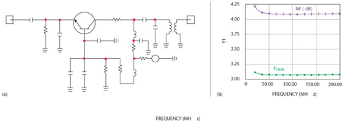
Figure 12 Buffer amplifier block diagram (a) and simulated noise figure and Fmin (b).
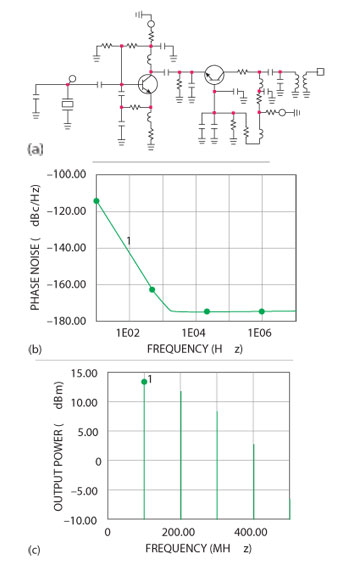
Figure 13 100 MHz crystal oscillator with the grounded-base amplifier (a), simulated noise figure (b) and power output plot (c).
Figures 14 through 17 show measured results from the 100 MHz crystal oscillator performed on systems from Agilent, Rohde & Schwarz, Holzworth and AnaPico, respectively. Appendix I (see online at www.mwjournal.com/synergyappendix) shows the phase noise calculation for this oscillator. The calculated 100 Hz offset phase noise is −146 dBc/Hz and the far out phase noise is − 183.3 dBc/Hz (see Figure 18). These numbers agree well with the R&S FSUP measurements. The Agilent results are close, but the system is not optimized as the “sweet-spot” has not been characterized. This may be frequency and power level dependent. The Holzworth equipment shows the best close-in correct phase noise level, but we have not found the proper correlation figures. The AnaPico test equipment seems to have a hump, but generally agrees well with the calculations. The Holzworth equipment performs the measurement in approximately 3 to 4 minutes (5 correlations), and about 1 minute with no correlations and 3 dB worse phase noise.
What does the law of physics tell us? As pointed out, here is the calculation for the Synergy LNXO100, SSB phase noise = Pout (dBm) + 177 (dB) – NF (large signal noise figure of the buffer amplifier). In our case, we get 14 + 177 − 7.7 =183.3. This means the SSB phase noise far out is −183.3 dBc/Hz.
Conclusion
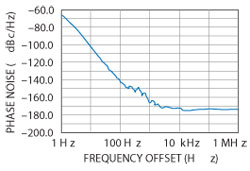
Figure 14 100 MHz crystal oscillator measured on Agilent E5052B (Corr_4000).
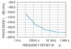
Figure 15 100 MHz crystal oscillator measured on R&S FSUP.
In this article, we have looked at typical oscillator circuits and some of their design rules. Calculations for phase noise were reviewed. Various systems were reviewed measuring a 100 MHz crystal oscillator. The phase noise equations give the best possible phase noise. If the equipment in use, after many correlations, gives a better number, it violates the laws of physics as we understand them and if it gives a worse number, then either the correlation settings need to be corrected or the dynamic range of the equipment is insufficient. We realize that this treatment is exhaustive, but we think that it was necessary to explain how things fall into place. At 20 dBm output, the output amplifier certainly has a higher noise figure, as it is driven with more power and there is no improvement possible. There is an optimum condition and some of the measurements showing -190 dBc/Hz do not seem to match the theoretical calculations. The correlation allows us to look below KT, but the noise contribution below KT is as useful as finding one gold atom in your body’s blood. This gold atom has no contribution to your system.
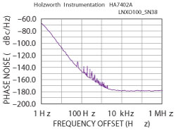
Figure 16 100 MHz crystal oscillator measured on Holzworth phase noise engine.
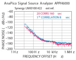
Figure 17 100 MHz crystal oscillator measured on AnaPico.
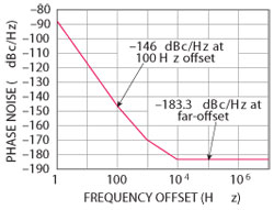
Figure 18 Calculated phase noise plot for 100 MHz crystal oscillator.
References
- U.L. Rohde, A.K. Poddar and G. Boeck, The Design of Modern Microwave Oscillators for Wireless Applications: Theory and Optimization, Wiley, New York, 2005.
- U.L. Rohde, Microwave and Wireless Synthesizers, Theory and Design, Wiley, New York, 1997.
- U.L. Rohde and M. Rudolph, RF/Microwave Circuit Design for Wireless Applications,Wiley, New York, 2013.
- U.L. Rohde, “Crystal Oscillator Provides Low Noise,” Electronic Design, 1975.
- G.D. Vendelin, A.M. Pavio, and U.L. Rohde, Microwave Circuit Design Using Linear and Nonlinear Techniques,Wiley, New York, 2005.
- A.L. Lance, W.D. Seal, F.G. Mendozo and N.W. Hudson, “Automating Phase Noise Measurements in the Frequency Domain,” Proceedings of the 31stAnnual Symposium on Frequency Control, 1977.
- Agilent Phase Noise Selection Guide.
- D. Calbaza, C. Gupta, U.L. Rohde and A.K. Poddar, “Harmonics Induced Uncertainty in Phase Noise Measurements,” 2012 IEEE MTT-S Digest, pp. 1-3, June 2012.
- U.L. Rohde, H. Hartnagel, “The Dangers of Simple use of Microwave Software,” www.mes.tu-darmstadt.de/media/mikroelektronische_systeme/pdf_3/ewme2010/proceedings/sessionvii/rohde_paper.pdf.
- “Sideband Noise in Oscillators,” 2009, www.conwin.com/pdfs/at_or_sc_for_ocxo.pdf.
- J. Cartwright, “Choosing an AT or SC Cut for OCXOs,” 2008.
- Benjamin Parzen, Design of Crystal and Other Harmonic Oscillators, John Wiley & Sons, 1983.
- U.L. Rohde and A.K. Poddar, Crystal Oscillators, Wiley Encyclopedia and Electronics Engineering, pp. 1-38, October 19, 2012.
- U.L. Rohde and A.K. Poddar, Crystal Oscillator Design, Wiley Encyclopedia of Electrical and Electronics Engineering, pp. 1–47, October 2012.
- U.L. Rohde and A.K. Poddar, “Latest Technology, Technological Challenges, and Market Trends for Frequency Generating and Timing Devices,” IEEE Microwave Magazine, pp. 120-134, October 2012.
- U.L. Rohde and A.K. Poddar, “Techniques Minimize the Phase Noise in Crystal Oscillators,” 2012 IEEE FCS, pp. 01-07, May 2012.
- E. Rubiola, Phase Noise and Frequency Stability in Oscillators, Cambridge University Press, 2009.
- http://ieeexplore.ieee.org/xpl/login.jsp?tp=&arnumber=4314363&url=http%3A%2F%2Fieeexplore.ieee.org%2Fiel5%2F19%2F4314356%2F04314363.pdf%3Farnumber%3D4314363.
- www.google.com/patents/US4797639.
- http://ieeexplore.ieee.org/xpl/login.jsp?tp=&arnumber=251295&url=http%3A%2F%2Fieeexplore.ieee.org%2Fiel1%2F58%2F6428%2F00251295.pdf%3Farnumber%3D251295.
- www.mentby.com/bruce-griffiths/notes-on-the-driscoll-vhf-overtone-crystal-oscillator.html.
- www.synergymwavegmbh.com/fileadmin/media/User_Files/SMR/pdf_files/SMR_Quartz_Phasenoise.pdf.