
This article presents a broadband, low-loss transition from rectangular waveguide (RW) to coplanar waveguide (CPW) at U-Band (40 to 60 GHz). The transition uses a transverse E-plane probe to get a wide bandwidth. The ground of the CPW is extended into the waveguide to obtain a well matched transition. The transition is implemented through a coupling to the waveguide bend, avoiding the inconsistency in the direction of signal transmission and facilitating the overall structure. A back-to-back (BTB) structure is used to demonstrate the feasibility of the transition. The reflection of a scalar network analyzer (SNA) affects the measurement results seriously. To solve this problem, this article performs an error analysis and offers an appropriate test method to reduce that influence. The return loss is measured with a matching load and the insertion loss is tested by adding a 20 dB attenuator between the device under test (DUT) and the detector of the SNA. The measured results of the BTB structure show that a return loss better than 20 dB and an insertion loss of 0.35 dB are achieved over the entire U-Band, which are close to the simulated results. The design had been used for a W-Band doubler and W-Band RW-to-CPW BTB transition.
CPWs on thin dielectric membranes are proved to have very satisfactory transmission properties, because of the absence of substrate modes, low losses and low dispersion.1 Due to RW’s low loss, simple topology, high-power handling capability and interconnect ability, it continues to be an important transmission line, especially in the millimeter-wave band.2 Thus, a transition between CPW and RW is needed, which should have a low insertion loss, a good return loss and a wide bandwidth.
Present reports about RW-to-CPW transitions use different forms of transition,3-5 but the probe transition is more attractive because of its low insertion loss, simple structure, tuning flexibility and broadband performance. Many articles have reported that using a transverse E-plane probe is the preferred method to achieve a wide bandwidth,6,7 but most of them are transitions from waveguide to microstrip. Other articles have introduced an extra structure, for example a stepped-impedance filter, used to suppress spurious radiation in unenclosed waveguide.5,8 This article improves these forms of transition, to design an enclosed simple broadband low-loss RW-to-CPW transition.
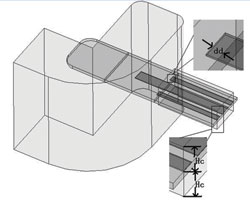
Figure 1 Model of the RW-to-CPW transition.
A vector network analyzer is difficult to obtain at U-Band or higher frequencies. An SNA cannot be calibrated to eliminate the detector’s reflection completely, which usually increases with frequency. Because of this, a measurement error analysis has to be discussed, but many articles ignore this analysis, resulting in significant difference between simulations and measurements.3,9,10 The measured reflection loss is worse than the simulation results by more than 5 dB and there is no reason given for this situation.3 In Xu Jun’s article,9 there are no measured results of return loss mentioned to verify the design. In Y.C. Shih’s article,10 there is a very large fluctuation, which is most likely caused by an incorrect test method, but no explanation has been made.
In this article, a RW-to-CPW transition at U-Band is proposed. This design makes some improvement to enhance its performance. The waveguide bend is coupled to avoid the inconsistency in the direction of signal transmission and make the overall structure suitable. The ground of the CPW, on both sides of the strip, is extended into the waveguide to make the transition well-matched. Finally, a BTB structure is used to evaluate its effect. In order to ensure the accuracy of the measurements, an analysis is performed on the influence of the reflection of the test equipment on measured results and offers an appropriate way to reduce this influence. This transition has been used in a W-Band doubler research and W-Band RW-to-CPW BTB transition study.
Design and Simulation of the RW-to-CPW Transition
Figure 1 shows the structure of the RW-to-CPW transition, which consists of a waveguide bend, an E-plane probe and a coplanar transmission line. The input waveguide is a standard R500 waveguide with inside dimensions of 4.775 × 2.388 mm.
The CPW Line and the CPW Channel
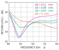
Figure 2 Simulated return loss as a function of dd.
The coplanar line is set in the middle of a channel and the bulk of the circuit operates in an enclosed region, so the CPW does not need some other structure to reject parasitic modes of the input signal, which is conducive to a miniaturized system. The fact that the electromagnetic field is distributed mostly in the air decreases greatly the dispersion and the loss is reduced.
The width of the CPW channel is certain, since the transition is designed for doubler applications at W-Band, which needs a standard R900 waveguide used as an output. Thus, the width is defined to be 1.270 mm based on the dimensions 2.540 × 1.270 mm of R900. Next, the height of the CPW channel (Hc) is set at 0.5 mm to avoid any waveguide mode by minimizing the height, while the CPW mode is not strongly affected. The impedance of the coplanar line can be maintained close to 50 Ω.
The Waveguide Bend
In a traditional E-plane probe transition, the input and output ports are perpendicular. To make them parallel, to solve the inconvenience of the structure, a waveguide bend is coupled to the transition. An important thing is that the inner angle cannot be fabricated by an existing processing technology. The RW is machined on the inside of a copper block. Considering these, the waveguide bend is manufactured with a round angle bend with an optimal radius of 3.05 mm and the two round corners at the back-short of the waveguide are designed with radius of 0.5 mm.
The Waveguide Probe
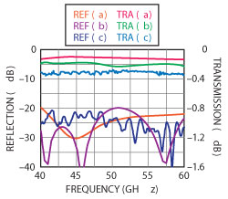
Figure 3 Simulated results (a) of the single transition and simulated and measured results of the BTB configuration.
The design of the waveguide probe is the most important feature of this approach. Using a transverse E-plane probe, which is inserted into the waveguide, can achieve a wider bandwidth. Besides, the waveguide probe is set away from the waveguide back-short approximately λg/4 at 50 GHz, which is approximately 1.6 mm. There are four parameters of the probe, all of which are simulated at various distances to each other except that the width and the length of the probe are not independent during the process, which also has to be optimized. Furthermore, the ground plane of the CPW line is extended a short distance into the waveguide to make a better match. Figure 2 shows the simulation results for different distances (dd), extended from the channel. It proves that the matching and the bandwidth of the transition can be further adjusted while the dd is changing. Finally, the distance is confirmed to be 80 μm.
The RW-to-CPW transition has been simulated. A BTB configuration is designed to facilitate the test. The final simulation results of the transition and the BTB structure are shown in Figure 3. The line (a) shows the simulations results of the single transition. The figure shows the transmission and reflection of the BTB transition, while (b) is the simulation results and (c) is the measured results. The simulations show that the transition achieves less than 0.15 dB insertion loss and the BTB configuration gets less than 0.25 dB, while both of them get a better than 20 dB rejection.
Measurement Error Analysis
Usually, a vector network analyzer is used in many situations. But it is difficult to obtain at U-Band or higher frequencies because of its high cost. Thus, the S-parameters over U-Band are tested most often with an SNA. The commonly used SNA has three detectors: one is used as reference through a power splitter, another is used to receive the reflected signal through a directional coupler, and the last is connected to the output port directly. Usually, the DUT’s performance is tested directly by connecting it with SNA. But, actually, there is not a perfect match between the DUT and the SNA’s detector. An SNA cannot be calibrated to eliminate the reflection, which usually increases as the frequency increases. It is clear that S-parameters, whether S11 or S21, are defined on the basis of the port match. When the reflection of the DUT’s load is large, the measurement results are away from its actual value, which would bring a large error.
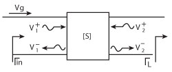
Figure 4 A two-port network.
Some analysis can be performed to explain this, which provides a precondition to obtain an appropriate test method. All the parameters are shown in Figure 4. V represents the voltage magnitudes at the ports and Vg represents the source voltage magnitude. When the DUT and the output load are mismatched, there is a load reflection coefficient which is assumed to be ΓL. The reflection coefficient seen from DUT’s input port to its load port is assumed to be Γin. The relationship between them is as follows:
Since the phase information cannot be obtained using an SNA, another equation is needed, which is just about the magnitude of the reflection coefficient. The final equation obtained from Equation 1 comes out as follows:

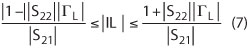
Equation 2 shows a circle in the complex plane with the center CL and the radius RL given below, in which Δ = S11S22 – S12S21.
From the equations above, the range of |Γin| can be known if |ΓL| is confirmed. When |ΓL| becomes smaller, the radius becomes smaller also. Only when |ΓL| is zero does |Γin| = S11. If |ΓL| changes from 1 to 0, it seems intuitive that CL will gradually close to S11 and RL will approach 0.
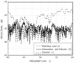
Figure 5 Reflection coefficient of a matching load (a), a 20 dB attenuator set before the detector (b) and the detector (c).
Figure 5 shows the reflection coefficients of different loads. It is obvious that the reflection of the matching load (a) and the 20 dB attenuator (b) are lower than that of the detector (c). The detector connected to the output port of DUT directly could seriously affect the measurement results of the BTB transition. Moreover, the reflection of the 20 dB attenuator presents more obvious peaks than the matching load. Thus, the reflection loss should be tested by a matching load connected to the output of DUT, which can make the measurement results close to its actual value.
In the same way, the insertion loss is to be analyzed to see how it is in-fluenced by the reflection coefficients of different loads. First, let us realize the definition of the insertion loss (IL) while the influence of the source is very small, which can be assumed to be zero. IL is the ratio of the output voltage amplitude of the signal source to that of the output port of the DUT after it is inserted.

In this formula, Vg is the voltage amplitude of source, just when the source is matched, and V2 is the amplitude of signal given to load. From the voltage relationship of two-port network, another equation can be obtained as follows:
When |ΓL| is zero, IL = –20 log |S21|. This equation also shows the range of |IL|.
The range of |IL| is also closely related to |ΓL| and |IL| is closer to 1/|S21| when |ΓL| becomes small.
The analysis proves that a lower load return loss makes the measured results more realistic. From Figure 5, it is found that the 20 dB attenuator has a lower reflection loss, so the load with the attenuator has a smaller effect on the measured results, compared with using the detector directly. Thus, a 20 dB attenuator, whose insertion loss can be eliminated by calibration, is set between the DUT and the detector of the SNA when the insertion loss is to be measured.
To understand the possible range of the measured error with different loads, the amplitude and phase of S-parameters of the BTB transition can be obtained from HFSS. Thus, the error range can be calculated and figured out with different reflection coefficient of loads, using the above equations. There are two examples where a specific frequency is assumed, such as 51.5 GHz. When |ΓL| = - 25 dB, that is 0.056, the reflection coefficient -27.5 dB ≤|Γin|≤-16.4 dB can be obtained from equation 2 and the insertion loss 0.2 dB≤IL≤ 0.3 dB from Equation 7. When ΓL = -18 dB, the reflection coefficient -28.4 dB ≤GΓin≤-13.6 dB and the insertion loss 0.14 dB≤IL≤0.36 dB are achieved. Comparing these two examples, it can be found that the measured reflection would be away from the real value when the reflection of the load is larger than that of the DUT. The insertion loss is in the same situation. This analysis will be proved in the measurements.
Measurements
The BTB configuration was fabricated in a copper block whose measurement results, shown in Figure 3, were taken with an Agilent 8757D SNA. By using the method proposed in this article, the influence of the reflection of the load that affects the measured results is decreased. The better the load and DUT match, the closer the measured results and actual values are. Even so, there is still an obvious difference between measured results and simulation results. This is because the influence of the load’s reflection is significantly improved, but not completely eliminated, especially when the practical reflection is very small.
Figure 3 shows that the insertion of the BTB transition is better than 0.35 dB with the curve changing slightly. The measurement of the return loss implies that a good performance in a wide band was achieved. The fractional bandwidth for the 20 dB return loss is greater than 40 percent, covering the whole operating frequencies of the U-Band.
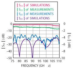
Figure 6 Simulated and measured results for the W-Band RW-to-CPW transition BTB configuration.
The analysis of the previous section shows that the measurements at one frequency have a difference in a certain range. Considering the processing and other factors, the final measurement of reflection loss, shown in Figure 3, is in line with the simulation results reasonably. Similarity, since the skin depth and the surface roughness are neglected, the measured insertion loss is slightly larger than the simulated one. Therefore, the measured results of insertion loss are in line with actual situation. Comparing these results with other published transitions,4-13 the measurement results of the BTB transition described here are much better than those given in papers where the reflection is worse than –15 dB, while the fractional bandwidth is less than 25 percent, or a 0.4 dB insertion loss can be found only in X-Band or near it. All these show that this approach uses a good configuration and an appropriate measurement method.
Because of the advantage of this transition, it has been used as the input part of a W-Band doubler, whose output is a R900 standard waveguide. This doubler uses parallel diodes to achieve frequency doubling and its best efficiency is approximately 6.4 percent at 40.5 GHz.
A W-Band RW-to-CPW transition’s BTB configuration is designed and measured based on the study in this article. A better than –15.65 dB reflection and a lower than 1.53 dB insertion loss are obtained, as shown in Figure 6. The actual insertion loss is better since the length of the back grounded coplanar transmission line is approximately 6.8 mm.
Conclusion
This article presents the design of a RW-to-CPW transition at U-Band. The transition achieves a low loss over a full bandwidth by using a transverse E-plane probe. In order to eliminate the parasitic mode, the coplanar line is clamped in the middle of the CPW channel and its enclosed structure does not need any filter. A waveguide bend is coupled to the transition to solve the inconvenience of the structure. To make the match much better between waveguide and CPW, the ground of the CPW line is extended slightly into the waveguide. Finally, a BTB structure is fabricated to verify the transition.
Since the reflection of an SNA’s detector cannot be eliminated by calibration, this article gives a measurement error analysis and proposes an appropriate method to achieve a more realistic measured value. The reflection is measured with a matching load connected to the output port of the DUT. The insertion loss is tested while a 20 dB attenuator is set between the DUT and the detector of SNA. A rejection of better than 20 dB and an insertion loss of 0.35 dB are achieved. The fractional bandwidth for the return loss is estimated to be 40 percent over the operating bandwidth. This transition has been successfully used in W-Band doubler and W-Band RW-to-CPW BTB transition.
References
- M. Riaziat, S. Bandy and G. Zdasiuk, “Coplanar Waveguides for MMICs,” Microwave Journal, Vol. 30, No. 6, June 1987, pp. 125-131.
- D.M. Pozar, Microwave Engineering, 3rd edition, John Wiley and Sons, 2005.
- V.S. Mottonen, “Wideband Coplanar Waveguide-to-Rectangular Waveguide Transition Using Fin-line Taper,” IEEE Microwave and Wireless Components Letters, Vol. 15, No. 2, February 2005, pp. 119-121.
- R.Y. Fang, C.T. Wang and C.L. Wang, “Coplanar-to-Rectangular Waveguide Transitions Using Slot Antennas,” IEEE Transactions on Components, Packaging and Manufacturing Technology, Vol. 1, No. 5, May 2011, pp. 681-688.
- T. Reck, R.M. Weikle and N.S. Barker, “A Waveguide to Unenclosed Coplanar Waveguide Transition,” IEEE Transactions on Microwave Theory and Techniques, Vol. 58, No. 9, September 2010, pp. 2420-2425.
- T.Q. Ho, Y.C. Shih and Y.C. Shih, “Spectral-domain Analysis of E-plane Waveguide to Microstrip Transitions,” IEEE Transactions on Microwave Theory and Techniques, Vol. 37, No. 2, February 1989, pp. 388-392.
- J.W. Kooi, G. Chattopadhyay, S. Withington, F. Rice, J. Zmuidzinas, C. Walker and G. Yassin, “A Full-Height Waveguide to Thin-film Microstrip Transition with Exceptional RF Bandwidth and Coupling Efficiency,” International Journal of Infrared and Millimeter Waves, Vol. 24, No. 3, March 2003, pp. 261-284.
- P. Soto, V.E. Boria, J.M. Catala-Civera, N. Chouaib, M. Guglielmi and B. Gimeno, “Analysis, Design and Experimental Verification of Microwave Filters for Safety Issues in Open-ended Waveguide Systems,” IEEE Transactions on Microwave Theory and Techniques, Vol. 48, No. 11, Part 2, November 2000, pp. 2133-2140.
- X. Jun, S.S Wang and M.Y. Wang, “Compact In-line Waveguide-to-microstrip Coaxial Probe Transition for Millimeter-Wave,” 2009 Asia Pacific Microwave Conference Digest, pp. 705-707.
- Y.C. Shih, T.N. Ton and L.Q. Bui, “Waveguide-to-Microstrip Transitions for Millimeter-Wave Applications,” 1988 IEEE MTT-S International Symposium Digest, pp. 473-475.