
Base station radio receivers convert high frequency signals at the antenna port to lower intermediate frequencies (IF) by mixing them with a local carrier signal. To detect weak signals in the presence of strong interferers, the receiver hardware requires a mixer function with low noise figure (NF) and high linearity. As the frequency of the received signal increases, it becomes a challenge to design mixers that meet the requirements of both loss and distortion simultaneously.
In the past decade, silicon integrated circuit (IC) downconverters, with built-in driver amplifiers and an integrated IF gain function, have emerged as the preferred solution to this system function. These ICs save cost and help make system operation more predictable and repeatable. The objective of this article is to explain the trend for this function being increasingly realized by manufacturers using BiCMOS technologies, and provide an overview of the key challenges that face the designer through a design example for base station receivers.
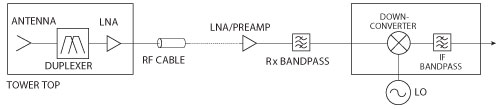
Figure 1 Typical RF input architecture of a base station receiver.
Downconverters: A Lumped, Discrete Component Approach Versus Fully Integrated Solutions
Most base stations for cellular infrastructure have low noise amplifiers at the tower-top, close to the antenna. The amplification of unwanted interferer tones as well as the signals of interest imposes tough linearity requirements on the downconverter. Conventional downconverters have used passive quad mixers (< 7 dB loss)1 driven by external local oscillator amplifiers (LOA). In a base station downconverter system, the mixer is followed by linear gain at the IF frequency, before the interfering tones are rejected by narrowband filters. The local oscillator signal requires significant boosting before it is applied to the mixer quad with typical drive powers greater than 20 dBm to achieve the required high linearity and low noise performance.
Whether the downconverter in Figure 1 uses either a single mixer (with an image reject pre-filter), or an IQ downconverter with a dual mixer function, the design challenges for both are identical. The composition of the mixer can be represented by the required functional blocks shown in Figure 2. The external 50 Ω LOA, IF amplifier, LO BPF and diplexer occupy a considerable area on the PCB, require many additional bias and matching components and increase the total variation in performance of the system parameters. This figure illustrates how the mixer is in fact comprised of several sub-function blocks – LOA, LO bandpass filter, diplexer, IF amplifier and a packaged 4 FET quad – with each block accounting for several components on the board. Ease of fabrication and test drives the selection of these to be 50 Ω single-ended components.
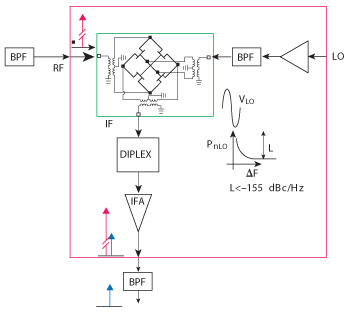
Figure 2 A conventional base station downconverter implementation.
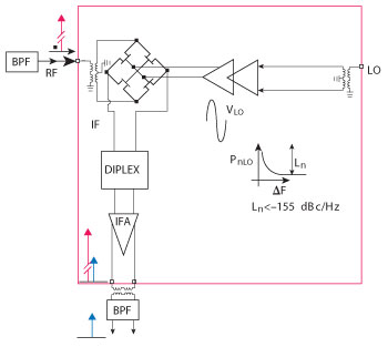
Figure 3 A Si IC downconverter encompasses all the high performance functions that make a downconverter in a base station.
Conversely, the integrated circuit downconvertershown in Figure 3 embeds all of these functions integrated within the silicon. Apassive quad-FET ring mixer, baluns, LOA, diplexer and IF amplifiers can be integrated into a single chip that fits within a 5×5 mm package enclosed within the red box. The freedom to choose optimum impedance levels and signal formats can then be leveraged in the IC design. The IF output can be made differential and therefore compatible with high quality differential surface acoustic wave (SAW) filter technology. In addition, signals can be transformed on-chip from their single-ended board representation into a differential format, which brings the benefit of providing intrinsic second harmonic suppression. Reference impedance levels can also be transformed, allowing the level of voltage swings at critical nodes in the circuit to be controlled and optimized, thus improving efficiency. Lastly, the differential drivers can be operated in a controlled and saturated state with minimal variation. This limiting behavior is conducive to achieving drive-independent performance specifications.
One approach that permits all of these functions to be integrated into a single small IC is to use a Silicon BiCMOS process technology that combines high performance, low noise, bipolar transistors for realizing the amplifiers, low-loss multi-layer transformers for baluns and a triple-well NMOS or NMOS-on-insulator device for the realization of the passive mixing quad.2
Modern technologies typically include multiple transistor types within a single process, where the speed (transition frequency ft) and BVCEO can be traded off against each other. Higher ft devices usually have a lower NF at the cost of a decreased breakdown voltage, which limits the maximum potential signal swing. However, commonly available devices with an ft of more than 100 GHz offer sufficient performance that can meet both the noise and distortion requirements in standard and cost-effective SiGe:C process technology.3
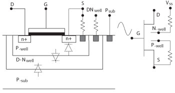
Figure 4 Triple-well NMOS used as a building block for four FET quad.
Silicon MOSFET devices used as passive switches, driven dynamically with the carrier signal, operate with low loss and importantly, low-distortion. Figure 4 illustrates a typical implementation of a triple-well NMOS device used in the passive mixing quad. The device cross-section shows a typical process implementation of an isolated NMOS device. The device is configured for use as a passive switch for use in a quad FET ring by the circuit representation on the right. The P-well is bootstrapped to the source to improve the available voltage swing and the deep N-well is reverse biased to further increase the isolation to the substrate by reducing the size of the depletion capacitance. The implanted deep N-well isolates the active P-well region of the NMOS device from the bulk substrate and this greatly reduced shunt capacitance has the effect of reducing signal loss at high frequency.
By keeping the D-N-well reverse biased, the impedance between P-well and D-N-well is increased (small intrinsic depletion capacitance), and the addition of a large resistor between the bulk and source node keeps the P-well floating at RF frequencies, thus enhancing linearity by reducing the diode clipping. The key parameters and the associated challenges facing the designer by means of a design example will now be reviewed.
BiCMOS FET-Based Mixer Design
A complex design problem can often be simplified or made more tangible by partitioning the problem into separate steps. This is especially true when the additional complication of frequency conversion is involved. In this example, the design is considered in four steps: the design of the mixer core, the design of the diplexer and sum terminations and the design of the two amplifier stages – the high linearity, low-noise differential IF amplifier and the driver amplifier used in the LO path.
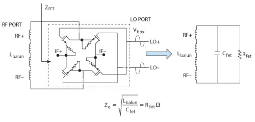
Figure 5 Simplified RF equivalent circuit of a fully driven and matched FET core.
Mixer Core Design
A high linearity FET mixer with a quad arrangement of NMOS devices driven by a large signal amplifier can be modeled for design purposes by the equivalent circuit shown in Figure 5. Assuming that the maximum allowable carrier swing (vLO = Vp cos (ωct)) at the LO port of the quad can be generated, the first step is to proceed to model the input impedance seen at the RF port. On-chip RF and LO baluns are used to convert single ended signals to differential signals at the input terminals of the FET ring. The peak swing of the LO drive signal, Vp, is selected to be as close to Vbox – the breakdown voltage of the FET device gate oxide – as possible to achieve high P1dB. The pumped N-FET quad can then be simply represented by a capacitance, Cfet in parallel with a resistance Rfet. The value of the capacitance Cfet is a function of the geometry of the FET device (W/L). The resistance Rfet originates from the dynamic switching of the mixer devices’ conductance. This pumped nonlinear conductance can be represented by the first term of a Fourier series expansion of the mixer’s time-varying conductance. The fundamental term responsible for the down-conversion, G1, is a function of both the LO drive amplitude, Vp, and the geometry of the NMOS device.
Mathematically, this time varying conductance, G (t), can be expressed as:
In a true double balanced mixer, the even harmonic terms are canceled. The input impedance of the mixer, as seen from the RF port, can therefore be modeled as the time-varying conductance of the FET-quad (with Rfet = 1/G1) in parallel with Cfet and the RF transformer’s magnetizing inductance Lbal.
It is important to ensure that the RF port of the mixer is well matched to the system source impedance for two reasons. First, as the input stage of the downconverter, the overall NF of the block will be dominated by the conversion loss of the mixing stage. Second, by providing a good matched load to the prior stage, it becomes easier to integrate the required image-reject or RF bandpass filters.
Ideally, this is equal to the characteristic impedance of the system at the frequency of operation (usually 50 Ω). However, by careful selection of both the device size (W/L) and the LO drive level such that Rfet = Zo, broadband performance is achievable from this circuit. The transformer loss is minimized and impedance matching is achieved by choosing Lbal and resonating with the capacitance of the NFET core (Cfet) such that:
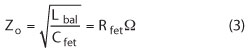
The mixer core in such a design can be thought of as having characteristic impedance, Zo equal to:
This model of the mixer core is used for the subsequent design steps.
Highly linear performance is achieved by fully driving the gates as close to Vbox as practical. A typical value in a 0.5 µm NFET technology, peak Vbox is typically approximately 6 V, although the full-drive is limited to 5 V for reliability reasons. For a given NMOS technology, the P1dB achievable for a fully-driven quad at various RF frequencies is a function of the device size within a given Zo environment.
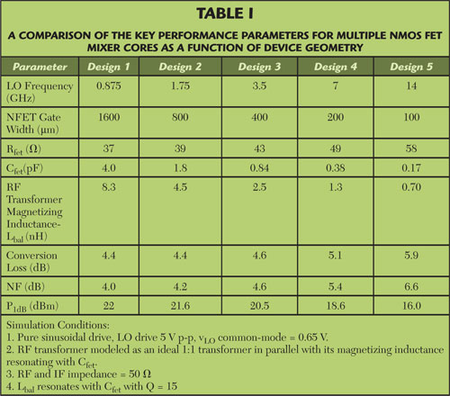
Equations 2 and 3 indicate that for a fixed system characteristic impedance, the operating frequency is inversely proportional to the equivalent capacitance of the mixer core. Therefore – all other things being equal – doubling the frequency of operation of the circuit necessitates halving the effective capacitance of the mixer core. The conclusion that therefore follows is that higher RF frequency mixers require shorter gate length devices to achieve low conversion loss, although the key parameter remains the matching of the time varying conductance of the mixer core to the characteristic impedance of the system at the optimum drive level. Table 1 shows how this approach may be used to scale a design within a specified technology for various operating center frequencies. This analysis is based upon the NXP QuBIC4X SiGe:C BiCMOS process with a 0.25 µm NFET. In this example, based on a typical technology, the peak-drive Vp < Vbox is approximately 2.5 V.
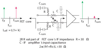
Figure 6 Principle and implementation of the diplexer design used to maintain maximum linearity from the IF amplifier.
Two observations can be made from the power-frequency table. For a given technology, the maximum P1dB achieved – with low conversion loss into a 50 Ω system – drops with increasing operating frequency. Increasing the W/L ratio (device periphery) at a given frequency not only yields lower conversion loss, but also allows more sweeping of dynamic conductance and hence achieves a higher P1dB. A lower Zo Ω mixer core, achieved by scaling Cfet and Lbal, can yield higher P1dB at peak LO drive.
Sum Termination and Diplexer Design
The four-FET quad mixer is a double sided mixer; both sum and difference frequencies are produced at the IF port at the same level. The signal of interest for the receiver (fLO – fRF or fRF – fLO for high-side or low-side injection respectively) is amplified inside the chip by the IF amplifier. However, the sum signal (fLO + fRF) is also generated and is incident upon the IF amplifier. The presence of this sum-signal will have the effect of deteriorating the dynamic performance of the downconverter, as the high frequency signal is reflected by the IF amplifier and re-mixed with the LO at the IF port. Therefore, to maximize the linearity of the downconverter, the sum signal should be rejected prior to the IF amplifier’s input. To prevent reflection of the sum signal and re-mixing with the LO at the IF port, the sum signal has to be absorbed4 by a termination. This can be achieved by incorporating a simple differential diplexer between the mixer and the IF stage to terminate the sum and pass the wanted difference signal with minimum loss.
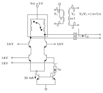
Figure 7 Transformer or tank resonated amplifier to generate voltage drives for nFET cores.
Figure 6 shows how the diplexer can be implemented with a simple highpass R-C section where the sum frequency is absorbed (terminated); R is half of the differential IF termination. A coupled series L connection tuned with the IF amplifier’s input capacitance (Miller capacitance for CE amplifier) works well to function as a low pass, high frequency reject section.
LO Driver Amplifier Design
The ability to drive the mixer core to present the correct dynamic conductance and optimize linearity requires optimizing the signal voltage swing at the FET quad. Signal voltage swings of 2.5 to 5 V translate to LO power levels of approximately 18 to 24 dBm, when referenced to a 50 Ω characteristic impedance. The magnitude of this LO voltage swing can be controlled in an IC implementation of the mixer quad-core by using a resonated amplifier technique,5 as shown in Figure 7. In this technique, the gate of the mixer quad is seen as a load that can be resonated by the tank connected to the open-collector of a cascode or CE differential BJT pair. A variant of this approach uses an n:n+1 transformer that can boost (step-up) the voltage drive into the mixer. This approach allows additional flexibility by allowing for the optimum LO signal swing at the mixer core to be treated somewhat separately to the peak signal magnitude at the output of the LO amplifier. In this example, SiGe HBTs are used in a cascode configuration to ameliorate the breakdown effects and improve the high-frequency performance.
Blocker and LO Noise Performance
The driver design in the last section emphasizes building up a large-signal to switch the NFETs at the local oscillator frequency. A large drive ensures linear operation of the mixer. While most driver designs address generation of large signals at the gate of the mixer, the noise performance of the drivers also need special attention.
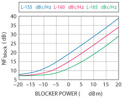
Figure 8 Noise figure under blocking conditions as a function of input blocking signal power and LO buffer noise.
In the presence of a large jammer at the RF port of the mixer, the noise at the local oscillator skirt will end up at the IF port due to reciprocal mixing.6 To minimize the signal-to-noise degradation, special care must be taken to design the LOA current source (Idc), whose low-frequency noise ends on both sides of the LO phase noise profile. The degradation of the noise figure due to jammers can be expressed in a closed form equation for an integrated circuit downconverter.7 NFblock is given as:
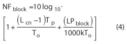
with L = 10(Ln /10), where Ln is the LO noise in dBc/Hz; Tp is the operating temperature; To = 290 K; Pblock is the blocker power in mW; k is the Boltzmann’s constant= 1.381310(-23)J/K and the conversion loss Lcn = 10(Lc/10), where Lc is in dB. Figure 8 shows how the noise figure (dB) of the downconverter under blocking conditions varies as a function of the input blocking signal power. The operating temperature in this plot is Tp = 25°C. It shows how the magnitude of the noise generated by the LO signal affects the total NF of the downconverter. Careful consideration of these plots give a guideline for the amount of allowable LO buffer noise (Ln in dBc/Hz) in the design so that the NFblock requirement can be met. The dominance of LO noise in determining the total signal-to-noise ratio degradation beyond Pblock = –5 dBm can be observed.
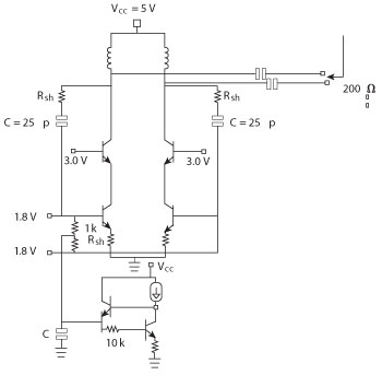
Figure 9 Series-shunt feedback cascode amplifier for superior band- width and reverse isolation.
Design of the IF Amplifier
The load network of the IF amplifier is a narrowband IF Filter (typically a surface acoustic wave (SAW) type) that are naturally differential. It is convenient for the output of the IF amplifier to be differential thus simplifying this interface connection. Figure 9 shows a series-shunt feedback cascade amplifier for superior bandwidth and reverse isolation. Series-shunt resistive feedback designs are common with the use of cascode configurations for broadband IF (50 to 800 MHz). High reverse isolation and low output capacitance of the high ft SiGe transistors and cascode amplifiers facilitate high (200 Ω) output impedances that match with the SAW filters.
The bias injection in the IF amplifier a) maximizes the headroom for output swing and b) minimizes the bias noise upconversion under blocking conditions. Base-ballasting and careful current mirror design ensures proper isolation between the bias circuit and IF. A capacitor C filters the noise and unwanted injections into the bias circuit. The classical tail current source is avoided for noise and headroom reasons.
SiGe BiCMOS Downconverter Design Example
The following example uses the steps outlined above to design a 2.5 to 3.5 GHz downconverter, fabricated using the NXP QUBiC4X SiGe
BiCMOS process from NXP.3 The 2.5 to 3.5 GHz RF frequency band is chosen for the design, due to its importance for LTE and WiMAX applications. With the model described in Design 3 of Table 1, the balun design is optimized to be centered at 3 GHz. The LOA design is optimized for fif = 300 MHz and a high-side injection LO (flo) band of 2.8 to 3.8 GHz is assumed.
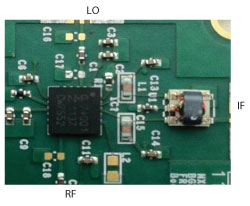
Figure 10 10 Photograph of the QFN-32, 5 × 5 mm packaged downconverter IC, designed using the principles and procedures outlined.
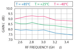
Figure 11 Conversion gain of the BGX7401 downconverter with nFET mixer and HBT IF amplifier.
The IC is packaged in an industry standard 5 × 5 mm QFN-20 plastic package as shown in the photograph of Figure 10. For characterization purposes, the differential IF port is transformed to a single-ended 50 Ω termination by means of a lumped external balun as seen on the extreme left of the image.
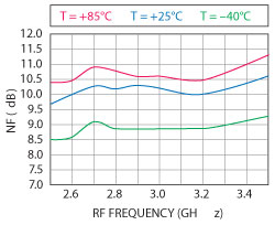
Figure 12 SSB noise figure of BGX7401 vs. RF frequency and temperature.
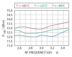
Figure 13 13 Input P1dB compression point of BGX7401 as a function of RF frequency and temperature.
The mixer IC draws 175 mA from a +5 V supply. With a typical IIP3 of +25 dBm and 8.5 dB gain and 10 dB noise figure, the measured results validate the design procedure outlined in this article. Typical gain, noise figure, P1dB and IIP3 measurements, as a function of both RF input signal frequency and ambient operating temperature (–40°, +25° and +85°C), are shown in Figures 11, 12, 13 and 14, respectively.
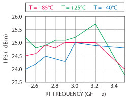
Figure 14 Input IIP3 vs. RF frequency and temperature.
Conclusion
A systematic design technique is shown that partitions the design problem into independent parts resulting in the dual-benefits of miniaturization and cost reductions. Old circuits simply do not die. They evolve and find their ways into newer designs with better performance. The design approach reviewed and implemented here takes a classic 4 FET quad and combines it with the benefits of small-size and high predictability, available from Si integrated circuit techniques. By also including the LO driver and IF amplifier functions in the integrated solution, higher efficiency circuits can be realized without compromising performance.
Acknowledgment
The authors acknowledge the help of Chris Bean and Andy Street of NXP Semiconductors with EV kit design and characterization. Kathiravan acknowledges the opportunity afforded by various design team managers at IBM and Maxim.
References
- Novel Passive FET Mixers Provide Superior Dynamic Range, Mini-Circuits Application Note AN00-003.pdf, www.mini-circuits.com.
- P. Park et al., “A High-Linearity, LC-Tuned, 24 GHz T/R Switch in 90-nm CMOS,” 2008 IEEE RFIC Symposium Proceedings, pp. 369-372.
- P. Deixler et al., “QUBiC4X: An ft/fmax=130/140 GHz SiGe:C-BiCMOS Manufacturing Technology with Elite Passives for Emerging Microwave Applications,” Proceedings of the 2004 Bipolar/BiCMOS Circuits and Technology Meeting, pp. 233-236.
- P. Will, “Reactive Loads – The Big Mixer Menace,” Microwaves, April 1971, pp. 38-42.
- D.K. Shaeffer and T.H. Lee, Low-Power CMOS Radio Receivers, Kluwer Academic Publishers, Boston, MA 1999.
- K. Krishnamurthi and S.P. Jurgiel, “Specification and Measurement of Local Oscillator Noise in Integrated Circuit Base Station Mixers,” Microwave Journal, Vol. 46, No. 4, April 2003, pp. 96-104.
- K. Krishnamurthi, Fundamentals of Radio Communications, Chapter 9: Noise in Radio Receivers, Adaiyalam Publishing House, India.