
A significant trend is the ever-increasing bandwidth requirements of high frequency electronics and modern data-transmission circuits, alongside a strong push toward integrated modules, is cost and performance. This means that classical coax connectors do not have an important role to play in large volume assemblies at high frequencies. However, connectivity solutions for test and measurement applications are required for frequencies up to 110 GHz and beyond in the design phase. To address these issues, the Solderless PCB Mount Rosenberger Precision Connectors (RPC) were developed.
Surface mount connectors are typically realized as right angle or edge mount types. Both of these types are used throughout the communication industry where impedance control and good shielding properties are required. They are reliable, exhibiting excellent and reproducible results. However, with the move to very high frequencies, where the wavelength of the transmitted signals is comparable to the dimensions of the connector, care has to be taken not to couple resonant structures to the signal path.
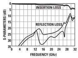
Figure 1 Calculated insertion (S12, S21) and reflection loss (S11, S22).
This means that careful control of potential resonances and radiation at the interface from the connector to the circuit board is essential for a predictable performance. The wavelength in vacuum is 3 mm at 100 GHz and quarter (0.75 mm) and half wave (1.5 mm) resonances have to be managed. Voids and gaps have to be small compared to these dimensions, keeping inmind that the wavelength is much smaller in the PCB dielectric.
Substrate Thickness
The substrate thickness also has to be kept well below a quarter wavelength for mode-free operation. The ratio of the width of a microstrip line and the substrate thickness is constant for a given substrate material. The sizes of millimeter-wave circuits are thus no more than a few tenths of a millimeter and have to be connected electrically by the center pin of the surface mount connector.
For illustration, we calculated the S-parameters of an edge mount connector that is shown in Figure 1. It shows excellent signal properties up to 25 GHz. However, a very strong resonance is observed at 30 GHz. This is caused by a parasitic resonant structure that is coupled to the transmission line via the gap between the connector body and the PCB ground. It sucks out a significant part of the signal, causing a deep narrowband dip in the order of several dBs in the insertion loss while causing a spike in the reflection loss.
A significant part of the signal is radiated into free space where it may potentially interfere with adjacent circuits. The logarithmic field plot of Figure 2 illustrates the resonant fringing field as it escapes through the void in the ground plane. Stressing a physical model, it behaves similarly to a waveguide transition with the signal pin acting like an inductive post. Let us consider how we mastered the challenges.
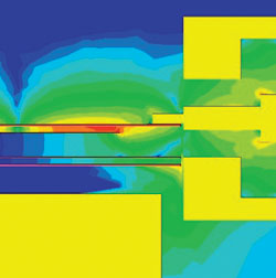
Figure 2 Field plot of the resonant fringing fields at 30 GHz.
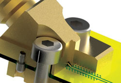
Figure 3 Detailed view of the PCB contact area with cut-out.
Technical Features
The structure of the connector topology that was chosen is depicted in Figure 3. The RF-ground plane and the top ground are connected by many vias that keep the PCB mode-free. The connector block is placed on top of the ground plane. This helps keep the footprint for this connector very simple and easy to design while no resonances may be excited in the transition.
The ‘pencil point’-like signal contact causes only a very low capacitive loading to the stripline, which is essential for minimum reflections at high frequencies. No voids are required in the ground plane that would otherwise make the design cumbersome. As the signal pin protrudes from the mounting face of the connector, a spring force is applied to the signal pad once the connector is mounted, providing a stable and vibration-proof connection.
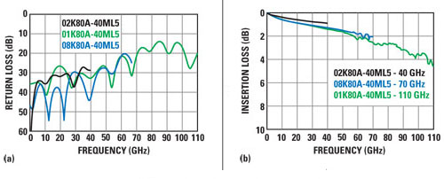
Figure 4 Measured reflection loss of solderless PCB mount connectors (a) and measured insertion loss (b).
Features
- Connectors are available in: RPC-2.92 (40 GHz) 02K80A-40ML5, RPC-1.85 (70 GHz) 08K80A-40ML5 and RPC-1.00 (110 GHz) 01K80A-40ML5
- No soldering required
- Prepositioning enforced by dowel pins
- Clamping mechanism accommodates a wide range of board thicknesses while providing a continuous ground connection between contact area and circuit board
- Universal, robust and reusable
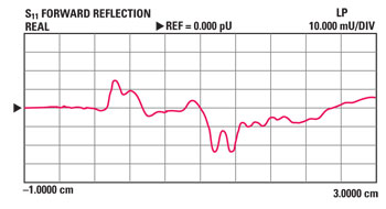
Figure 5 Gated S11 in TD of the 110 GHz connectors 01K80A-40ML5.
As expected from the simulations, test results confirm the excellent RF-properties of the new connector series with connectors available up to 40, 70 and 110 GHz. Reflection loss and insertion loss of the three products are plotted in Figures 4a and 4b, respectively. The frequency response is mode-free up to 110 GHz. The insertion loss represents 50 percent of the GCPW-losses on the PCB. The actual insertion loss of the connectors is considerably lower. The 70 and 110 GHz versions have been tested on the same substrate. A separate design was chosen for the 40 GHz version.
This explains the lower loss of the 02K80A-40M at lower frequencies. It may be attributed exclusively to the different PCB layouts. The TDR response of the 110 GHz type of connector is shown in Figure 5. The coaxial interface is on the left. It confirms the excellent impedance control along the signal path. There is a wide field for the application of this connector family in the ultra high frequency test and measurement applications and also in situations where minimum radiation and coupling to adjacent circuitry is mandatory.
Rosenberger Hochfrequenztechnik GmbH & Co. KG,
Fridolfing, Germany
+49 (0) 86 84 180,
info@rosenberger.de
www.rosenberger.com