

Today’s radio designs, and other RF communication equipment, are being made to consume less power while occupying less physical space, which leads to less available board area for heat sinking. In addition, these systems are being deployed in more extreme environmental conditions where only passive cooling is being used, which leads to the need for very reliable ICs that can withstand greater temperature variations. When the factor of system output power scalability gets added in, the need emerges for new equally scalable RF driver amplifiers. To satisfy all of these goals, Analog Devices has re-characterized the ADL5320 and ADL5321 ¼ W SOT-89 driver amplifiers for 3.3 to 5 V operation, as well as –40° to 105°C operation. The ¼ W drivers are now characterized in the same way as the newly released ADL5324 ½ W SOT-89 driver amplifier.
Analog Devices’ driver amplifiers incorporate a dynamically adjustable biasing circuit that allows for the customization of OIP3 and P1dB performance from 3.3 to 5 V, without the need for an external bias resistor. This feature gives the designer the ability to tailor driver amplifier performance to the specific needs of the design. The adjustable bias also allows for the drivers to be dynamically biased in order to conserve power consumption when the full performance of the driver amplifier is not required, such as when a system is in standby mode. This scalability reduces the need to evaluate and inventory multiple driver amplifiers for different output power requirements, from 22 to 27 dBm output power levels for the ¼ W drivers, and from 24 to 29 dBm output power levels for the ½ W driver. The three drivers are also rated to operate across the widest temperature range of –40° to +105°C for reliable performance in designs that will experience higher temperatures, such as power amplifiers. The two ¼ W drivers, and the ½ W driver amplifier, cover the wide frequency range of 400 to 4000 MHz and only require a few external components to be tuned to a specific band within that wide range. These high performance broadband RF driver amplifiers are well-suited for a variety of wired and wireless applications including cellular infrastructure, ISM band power amplifiers, defense equipment, and instrumentation equipment.
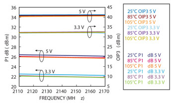
Figure 1 ADL5320 OIP3 and P1dB performance vs. voltage bias.
The ADL5320 GaAs HBT ¼ W driver amplifier operates from 700 to 2700 MHz, and consumes a low 5 V current of 104 mA. When operated at 5 V, the ADL5320 delivers a high level of performance at 880 MHz with an OIP3 of 45 dBm, a P1dB of 25.4 dBm, a gain of 16.9 dB and a low noise figure of 4.1 dB. When the bias voltage is reduced to 3.3 V, the driver only consumes 44 mA and delivers an OIP3 of 34 dBm, a P1dB of 21.5 dBm (see Figure 1), a gain of 15.6 dB, and a lower noise figure of 3.2 dB at 880 MHz. The driver amplifier can also be biased anywhere from 3.3 up to 5 V to meet system needs that are in between the performance stated at 3.3 or 5 V. This feature creates the opportunity for dynamic biasing of the driver amplifier where a variable supply is used to allow for full 5 V biasing under large signal conditions, and then reduced supply voltage when signal levels are smaller and lower power consumption is desirable. The driver can deliver 16 dBm of output power at 2140 MHz, while achieving an ACPR of –55 dBc at 5 V. If the bias is reduced to 3.3 V the –55 dBc ACPR output power only minimally reduces to 9 dBm (see Figure 2).
The ADL5321 GaAs HBT ¼ W driver amplifier operates from 2300 to 4000 MHz and consumes a low 5 V current of 90 mA. When operated at 5 V, the ADL5321 delivers a high level of performance at 2600 MHz with an OIP3 of 41 dBm a P1dB of 25.7 dBm, a gain of 14 dB, and a low noise figure of 4 dB. When the bias voltage is reduced to 3.3 V, the driver only consumes 37 mA and delivers an OIP3 of 31 dBm, a P1dB of 22 dBm, a gain of 12.6 dB and a lower noise figure of 3.5 dB at 2600 MHz. The driver amplifier can also be biased anywhere from 3.3 up to 5 V with its dynamically adjustable bias.
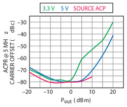
Figure 2 ADL5320 ACPR performance vs. voltage bias.
The ADL5324 GaAs HBT ½ W driver amplifier consumes a low 5 V current of 133 mA and also delivers very high performance at 2140 MHz with an OIP3 of 43.1 dBm, a P1dB of 29.1 dBm, a gain of 14.6 dB and a low noise figure of 3.8 dB. When the bias voltage is reduced to 3.3 V, the driver only consumes 62 mA and delivers an OIP3 of 34.4 dBm, a P1dB of 25.3 dBm, a gain of 13.6 dB and a lower noise figure of 3.2 dB at 2140 MHz. The driver amplifier can also be biased anywhere from 3.3 up to 5 V with its dynamically adjustable bias. The driver can deliver greater than 17 dBm of output power at 2140 MHz, while achieving an ACPR of –55 dBc at 5 V. If the bias is reduced to 3.3 V, the –55 dBc ACPR output power only minimally reduces to 15 dBm.
The three drivers further simplify RF design by eliminating the need for complicated external tuning. The drivers only use 50 Ω lines at the input and output of the amplifier, and also do not require an external bias resistor. The drivers only need one shunt capacitor at its input and one shunt capacitor at its output for frequency tuning. The usual AC coupling capacitors and DC bias choke inductor are also required, along with the standard bypass capacitance on the DC bias trace.
The driver amplifiers were also designed and packaged to simplify thermal considerations. The drivers have very low current consumption at either 3.3 or 5 V, which reduces the amount of heat that is created. The standard SOT-89 package also has a large backside ground paddle that allows for an efficient thermal transfer path from the amplifier. The datasheets show the recommended circuit board land pattern with added thermal transfer vias to further improve thermal transfer characteristics. This allows the driver to be kept within safe operating temperatures without the need for forced air cooling, and the driver is fully specified over the widest operating temperature range of –40° to +105°C. The drivers are also rated to a minimum HBM ESD rating of ±2 kV (Class 2), which makes it equally robust in high volume manufacturing environments.
Another way Analog Devices helps improve RF design is with the amount of information provided in the company’s datasheets. Data provided, such as critical parameter variation versus temperature, from –40° to +105°C, voltage supply, from 3.3 to 5 V, and operating frequency, from 400 to 4000 MHz, reduces the amount of qualification time a designer needs to spend. That reduction in qualification time can significantly improve a projects’ time-to-market. The comprehensive datasheet also allows the designer to accurately determine the least amount of power consumption achievable to meet the performance goals for his or her given application.
Analog Devices improves RF design in multiple ways: through innovative circuit design, simplified tuning requirements, and detailed datasheet information. These attributes allow RF designers to go to market quickly with solutions that meet their needs for smaller, lower power consuming systems.
Analog Devices Inc.,
Norwood, MA,
www.analog.com