
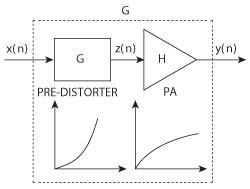
Figure 1 Pre-distortion system.
Designers transitioning 3G systems to 3.9G and 4G to keep pace with emerging devices like smartphones, face a number of critical obstacles. As an example, consider that signals in advanced wireless communication systems (such as LTE-Advanced and 802.11ac signals) are wideband and have a high peak-to-average power ratio (PAPR), that is, large fluctuations in their signal envelopes. Because of this, the power amplifier (PA) must be backed off well below its maximum (“saturated”) output power, in order to handle infrequent peaks, which results in very low efficiencies, typically less than 10 percent. Luckily, power amplifier linearization techniques offer designers one means of increasing power efficiency. One such method, digital pre-distortion (DPD), linearizes the nonlinear response of a PA over an operating region. It uses digital signal processing techniques to condition a baseband signal prior to modulation, up-conversion and amplification by the PA. Using DPD, designers can achieve high efficiency and avoid the severe distortion caused by PA nonlinearities.
While DPD offers an extremely cost-effective way to accomplish linearization, its use often requires a highly specialized skill set for modeling and implementation. Moreover, the traditional means of extracting a DPD model requires the PA to be turned ON and OFF, when switching to accurately capture PA input and output. Additionally, it supports PA DPD verification only. For linearization of the full RF transmitter, including ADC, filter, amplifier, up-converter and PA, a more novel DPD measurement method is required.
Understanding DPD
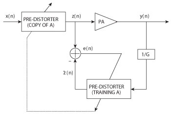
Figure 2 Indirect learning pre-distortion scheme.
The principle of a digital pre-distorter, shown in Figure 1, is intrinsically simple. A nonlinear distortion function is built up within a numerical or digital domain that is the inverse of the distortion function exhibited by the amplifier. The predistorter (PD) is designed for some linearization criteria — typically, the suppression of adjacent channel power — while also working to minimize power consumption. Because the PD must be as good an inverse of the PA response function as necessary and compensate for PA deficiencies like nonlinearity, memory effects and gain drift, its design requires good knowledge of the PA’s behavior. The PD-PA cascade attempts to combine two nonlinear systems into one linear result, which allows the PA to operate closer to saturation.
Memory Polynomial DPD
One popular DPD solution commonly employed by the industry is the memory polynomial DPD. To better understand this algorithm, consider Figure 2, which shows the indirect learning architecture for the digital pre-distorter. The feedback path labeled “Predistorter Training” (block A) has y(n)/G as its input, where G is the intended PA small signal gain and Ẑ(n) as its output. The actual pre-distorter is an exact copy of the feedback path (copy of A) with x(n) as its input and z(n) as its output. Ideally, y(n) = Gx(n), which renders z(n) = Ẑ(n) and the error term e(n) = 0. Given y(n) and z(n), this structure enables the parameters of block A to be directly found, yielding the pre-distorter. The algorithm converges when the error energy ||e(n)||2 is minimized.
The DPD architecture in the figure illustrates the case where x(n) is the input signal to a pre-distortion unit whose output z(n) feeds the PA to produce output y(n). The most general form of nonlinearity with Q+1-tap memory is described by the Volterra series, which consists of a sum of multidimensional convolutions. In the training branch of the figure, the Volterra series pre-distorter can be described by:
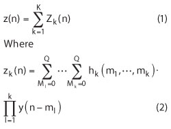
is the k-dimensional convolution of the input with Volterra kernel. This is a generalization of a power series representation with a finite memory of length Q+1. The z(n) also can be written as follows:
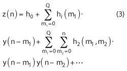
A memory polynomial pre-distorter uses the diagonal kernels of the Volterra series and can be viewed as a generalization of the Hammerstein pre-distorter. It is used to linearize PAs with memory effects. The memory polynomial pre-distorter is constructed using the indirect learning architecture, thereby eliminating the need for model assumption and parameter estimation of the PA. Compared to the Hammerstein pre-distorter, the memory polynomial pre-distorter has slightly more terms; however, it is much more robust and its parameters can be easily estimated by way of least-squares.
The memory polynomial pre-distorter can be described as:
where y(n) and z(n) are the input and output of the pre-distorter in the training branch, respectively, and akq denotes the coefficients of the pre-distorter.
Because the model in Equation 4 is linear with respect to its coefficients, the pre-distorter coefficients can be directly obtained using a least-squares approach by defining a new sequence:
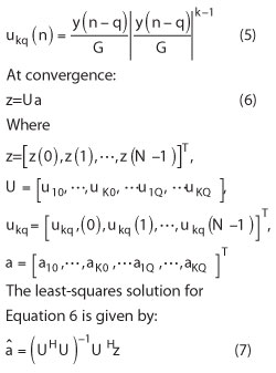
where (·)H denotes the complex conjugate transpose. Once the memory polynomial coefficients are obtained,
they can be loaded into the nonlinear filter in the memory polynomial to create a working memory polynomial pre-distorter.
PA DPD Verification
The behavior of the pre-distorter or device-under-test (DUT) can be experimentally measured using the instantaneous complex baseband waveform approach. This traditional means of extracting a DPD model relies on both PA input and output and needs to switch to capture the necessary PA input and output. Sometimes, the PA must be turned ON and OFF when switching.
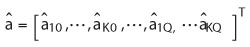
Figure 3 Experimental instrument platform for PA and DPD modeling.
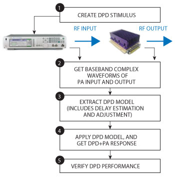
Figure 4 Behavior model extraction procedure with both PA input and output.
A typical setup for this traditional approach is shown in Figure 3. Here, the digital baseband waveform is downloaded to a vector signal generator (VSG) that feeds the PA (that is the DUT) with the corresponding RF modulated signal. The output of the DUT is then down-converted and sampled by a vector signal analyzer (VSA). Finally, the sampled input and output data is captured and used to extract behavioral models (both DPD and PA) for the PA. To accurately observe the behavior of the DUT, the instruments in the setup must have an appropriately large dynamic range and bandwidth.
As shown in Figure 4, the typical design flow for extracting DPD and PA models using both the PA input and output is as follows:
Step 1. The DPD stimulus waveform (that is 802.11ac, LTE/LTE-A, WCDMA, or user defined) is created and downloaded via LAN or GPIB into the VSG.
Step 2. The PA’s response, both input and output (point B and A in Figure 3), is captured from the VSA running vector signal analysis software. The PA output signal is captured by inserting the PA between the VSG and VSA with appropriate signal calibration, including any signal padding with attenuators.
Step 3. DPD models are extracted based on PA input and output. This includes time delay estimation and adjustment. Note that the propagation delay through the DUT introduces a mismatch between the data samples used to calculate the instantaneous AM/AM and AM/PM characteristics of the DUT. This mismatch translates into dispersion in the AM/AM and AM/PM characteristics, which can be misinterpreted and considered as memory effects.
Step 4. The DPD+PA response is captured by applying stimulus to the extracted DPD model and downloading the DPD output waveform into the VSG. The PA output waveform is then captured from the VSA.
Step 5. The DPD+PA response is verified, and the performance improvements possible with DPD can be shown.
This traditional method is effective in providing DPD with a specific PA; however, it does have some drawbacks. Because it requires switching, for example, the method is complicated. It can also be tiresome and dangerous to continually turn the high power amplifier ON and OFF. The distortion characteristic will be different after each turn OFF and ON, impacting both DPD model extraction and DPD performance. Additionally, the method fails to provide a DPD for the full analog circuit board, something that is recommended given that in actual application, the DAC, up-converter, pre-amplifier and PA are all designed on one analog circuit board.
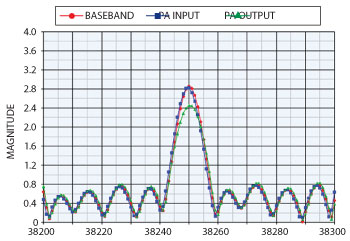
Figure 5 Sample time-domain waveform of baseband input, PA input and PA output.
The Full RF Transmitter Linearization Method
In contrast to the traditional approach to PA DPD verification previously detailed, DPD models can also be extracted using simulated baseband input and real PA output. In this case, a baseband input waveform replaces the PA input waveform in Figure 3 (that is Point C replaces Point B). Rather than just supporting PA DPD verification, this method provides a DPD verification solution for the full RF transmitter, including ADC, filter, amplifier, up-converter and PA.
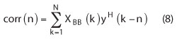
The full RF transmitter linearization method follows the steps previously detailed for PA DPD verification with one exception. Additional coarse time-delay estimation performed at the sample level is required in Step 2 to synchronize between the real PA output waveform and the simulated baseband waveform. This is done because a trigger signal is used to capture the arbitrary waveform from the VSA and the baseband waveform, which is the ideal waveform and, therefore, does not have any time-delay. The coarse time delay is estimated according to the cross-covariance between the input and output sequence of the PA as follows:
where N is the number of captured samples.
Following the coarse time-delay estimation, a fine time-delay estimation is carried out by placing a higher interpolation rate between the PA output and baseband waveform. This fine time-delay estimation is the same as the algorithm used between the PA output and input waveforms.
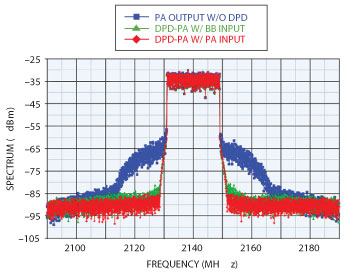
Figure 6 Spectrums of the system with and without DPD.
This method for full RF transmitter linearization can correctly extract a DPD model for the VSA, pre-amplifier and PA when the VSA works without nonlinear distortion. Figure 5 shows the normalized magnitudes of the time-domain waveform of the baseband waveform, PA input (or VSG RF output) and PA output after coarse synchronization (sample-level synchronization). Note that for this measurement, the VSG’s RF power should be small enough to allow the PA to work on a linear area. If not, the DPD model extraction will fail.
In contrast to the PA DPD verification method, this method provides DPD for the full RF system and does not need to switch to capture PA input and output or turn the PA ON and OFF. The high-power amplifier can always be turned ON during DPD verification. Moreover, the pre-amplifier and the high-power amplifier are designed in an analog circuit board.
Comparing DPD Verification Methods
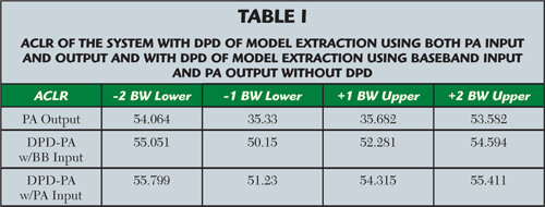
To compare the DPD performance associated with using the two DPD verification methods presented (that is with PA input or with baseband input), consider Figure 6, which shows LTE DL 20-MHz DPD performances with a Mini-Circuit 1-W PA. The blue line is the spectrum of the PA output, while both the red and green lines are spectrums of the PA with DPD. The red line is spectrum with PA input and PA output extraction. The green line is spectrum with baseband input and PA output extraction. Table 1 shows ACLR results of the PA output, DPD-PA with PA input and DPD-PA with baseband input.
From Figure 6 and Table 1, it is possible to see that the performance of the DPD-PA with PA input (red) is better than that of the DPD-PA with baseband input (green). The green spectrum is the DPD result with a full RF transmitter system. The DPD needs to remove the nonlinear distortion of the ADC and preamplifier, as well as the PA. The red spectrum is the DPD result with the measured PA.
Conclusion
Power amplifier linearization remains an important technique for current and emerging advanced communication systems. DPD verification can be accomplished using one of two methods. The more traditional approach uses an instantaneous complex baseband waveform and both PA input and output to extract a DPD model for a specific PA. A more novel approach extracts the DPD model by using a simulated baseband input and real PA output. This method eliminates the shortcomings of the more traditional method, allows designers to obtain high efficiency and avoid distortion caused by PA nonlinearities and also enables full RF linearization.
Jinbiao Xu received his Bachelor’s Degree in Mathematics, Master’s and Ph.D. degrees in information engineering from Xidian University at Xi’an, China in 1991, 1994 and 1997, respectively. From 1997 to 1998, he was a postdoctoral researcher on low speech codec investigation at the Institute of Acoustics, Chinese Academy of Science. Since joining Agilent EEsof EDA in 1999, he has been responsible for the OFDM series wireless library development (including DVB-T, ISDB-T, IEEE802.11a, WiMedia, mobile WiMAX and 3GPP LTE). His current responsibility is to implement digital pre-distortion, MIMO channel model, custom OFDM, etc. His research interests include MIMO, OFDM, pre-distortion and satellite communications.