
In wireless receivers, limiters prevent large incoming signals from momentarily overdriving or permanently damaging the sensitive front end stages such as the low noise amplifier (LNA) and the mixer. In a transmitter, the limiter is used to curtail modulation peaks from exceeding the power amplifier’s input limit. The simplest limiter circuit consists of a PIN diode and a parallel inductor for DC return – the “self-biased limiter.” When the incoming signal amplitude exceeds the PIN diode’s turn-on voltage, rectification occurs, and the resultant circulating current biases the diode to a low impedance state that reflects the signal back to the source. The input power at which the limiter has a 1 dB higher loss than its quiescent state is defined as the limiting threshold. Using a PIN diode with 1.5 µm thick I-layer in this limiter achieves a limiting threshold of approximately 10 dBm,1 but this is higher than what many LNA devices can tolerate. Adding a Schottky diode in anti-parallel to the PIN diode creates the Schottky-enhanced PIN limiter, which favorably lowers the limiting threshold by approximately 8 dB2-3 because of the Schottky diode’s lower turn-on voltage. Moreover, the addition of the faster Schottky diode speeds up the limiter’s turn-on time.4 The Schottky-PIN limiter does not require a shunt inductor because the anti-parallel diodes form a complete DC path. Consequently, the absence of the shunt inductor is encouraged to improve both bandwidth and loss in the anti-parallel configuration.5
The recovery time is the period during which the limiter gradually returns to a low-loss state following the cessation of overdrive. This transitory state, which is also known as the blind/dead time, disrupts communication and causes information loss. In nuclear magnetic resonance and magnetic resonance imaging, slow recovery in the “crossed diodes” RF-actuated switch – which is essentially a limiter – creates imaging artifacts.6-7 The recovery time of the self-biased PIN limiter is extensively described in the literature – it is proportionate to the PIN diode’s I-layer thickness8 and is approximately equal to the diode’s minority carrier lifetime Tau.9-10 In contrast, there is a dearth of information pertaining to the recovery time of the PIN-Schottky limiter despite this topology’s increasing popularity, as shrinking transistor dimensions necessitates lower limiting thresholds than before. This study of the PIN-Schottky limiter’s recovery characteristics was performed because quantitative data was not found elsewhere. This article documents the results of measurements on the most popular form of the PIN-Schottky limiter and also proposes a simple modification to speed up the recovery time.
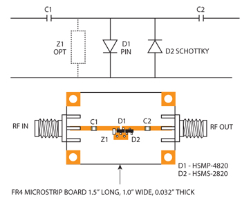
Figure 1 PIN-Schottky limiter circuit diagram and printed circuit board assembly.
Materials and Methods
This section describes the components that form the evaluated limiter and then the measurement setup. The prototype for the recovery time evaluation, shown in Figure 1, follows a circuit arrangement intended for reducing high frequency losses caused by the diode parasitic capacitances.2 The PIN limiter diode D1 was chosen for the following reasons: a relatively thin 1.5 µm I-layer to achieve fast transient response and 100 µm diameter to handle up to 10 W incident power.11-12 The detector diode D2, formed of a Schottky and a PIN hybrid, was chosen for a compromise of robustness (>15 V breakdown voltage) and sensitivity (250 mV barrier height at 1 mA bias).13 The diode chips are connected by bond wires at the top and conductive epoxy at the bottom to their lead-frames. The lead-frames are then epoxy molded to form SOT-23 packages. The packaged diodes and two DC blocking capacitors (C1, C2) are soldered to 50 Ω microstrip traces on a FR4 printed circuit board measuring 1.5" × 1" × 0.032." Following the previous authors’ assertion that the anti-parallel arrangement eliminates the low frequency limit imposed by the shunt inductor, a relatively large capacitance value of 1 nF was initially chosen to enable operation down to the tens of MHz range. RF connections to the PCB are made via two edge-launch SMA connectors (Johnson 142-0701-881).
The limiter’s recovery from an overload pulse is measured using a two frequency method first proposed by Goldie in 196714 and subsequently re-discovered and updated with modern test accessories by Looney, et al. in 2004.15 In this method, the separation of the overdrive pulse and the much weaker desired signal in the frequency domain allows the limiter’s response to the latter to be isolated using simple filters (see Figure 2). The original X-Band test frequencies were transposed to the VHF-UHF range to suit the plastic packaged diodes’ lower useable frequency range. The desired signal S1 is a 200 MHz, –5 dBm continuous wave. The incident overdrive S2 consists of a 10 µsec burst of 900 MHz, 30 dBm carrier. The frequency spacing between S1 and S2 is arbitrary – it is chosen to ensure the 200 MHz low pass filter (Mini-Circuits SLP-200) in front of the detector has sufficient rejection of the 900 MHz pulse. Both signals are combined in a directional coupler, because the isolation between its main and coupled branches can prevent cross modulation – a hybrid combiner can also be used in the same slot, if available. Since PIN junction heating is known to significantly increase the measured recovery time,9-10 the overdrive signal is pulsed at 10 µsec bursts and the incident power is roughly one-tenth of the limiter’s maximum power handling. To permit visualization of the limiter’s output waveform on an available 150 MHz oscilloscope, the waveform’s envelope is extracted using a commercial low barrier Schottky diode detector (Agilent 8473C). The detector output terminal is loaded with a 50 Ω resistor in order to achieve a sufficiently fast response time16as required by this test.
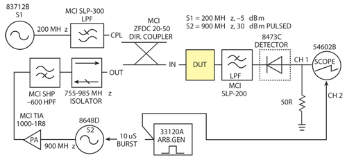
Figure 2 Test setup for recovery time.
Results and Discussion
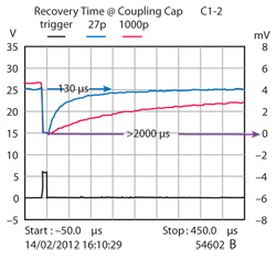
Figure 3 PIN-Schottky limiter recovery time as a function of blocking capacitance value.
This section first presents the results obtained from the standard PIN-Schottky limiter circuit and then the results following different modifications. The PIN-Schottky limiter’s recovery from overload is extremely slow because it is dependent on surrounding components, which have relatively large RC time constants. The results reveal that the DC blocking capacitances are the primary determinant of the limiter’s recovery time. For the 1 nF and the 27 pF capacitances evaluated, the corresponding recovery times are 2000 and 130 µsec, respectively (see Figure 3). These results are several orders of magnitude larger than the < 70 nsec recovery time of a self-biased PIN limiter using the same diode type. The self-biased PIN limiter owes its fast recovery to the requisite shunt inductor. On the other hand, the inductor absence from the PIN-Schottky limiter means the positive voltage stored in the capacitors can continue to bias the PIN diode long after the overdrive has ended. The observation of slower recovery with larger capacitances is due to the larger stored charge. Therefore the bandwidth improvement in the anti-parallel topology is a double edged sword, because it can only be achieved at the expense of a very slow recovery. The unacceptably slow recovery may have escaped previous authors’ attention because the two-frequency measurement method was not well known prior to 2004. Additionally, wireless traffic before 2G was mostly voice-based – so, a recovery period of a few milliseconds may have been below the audibility threshold. In radar applications, the recovery period corresponds to echoes from nearby targets and so a higher insertion loss may be tolerated.10
The PIN-Schottky limiter’s recovery time can be reduced by three orders of magnitude or more by the addition of a ground return path in the form of either an inductor or a resistor (Z1 in Figure 1). Of course, reintroducing the ground return cancels the anti-parallel diode configuration’s bandwidth advantage. Retaining the 1 nF capacitors in the evaluated limiter, the recovery times are reduced to 0.2 nsec and 2 µsec with the addition of a 100 nH inductor and a 1 kΩ resistor, respectively (see Figure 4). These component values are chosen to provide sufficient choking at the test frequencies. However, the inductor’s speed advantage is marred by a large spike at the leading edge of the recovered waveform. Because the spike peak has almost twice the amplitude of the flat recovery, the inductor’s under-damped solution may be unacceptable to sensitive applications. The 1 kΩ shunt resistor achieves critical damping –resulting in a spike-free leading edge although at the cost of a ten times slower recovery than the inductor. A 220 Ω resistance has a recovery time in between that of the inductor and the 1 kΩ resistor, but it is not recommended because the flat recovery voltage is 31 percent lower (3.4 vs. 4.9 mV), and this portends to a higher small signal loss.
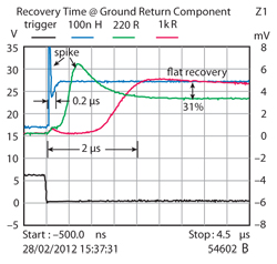
Figure 4 Limiter recovery time as a function of ground return component Z1.
Conclusion
The PIN-Schottky limiter’s recovery time is determined by its external components rather than by the diode minority charge carrier as in the self-biased PIN limiter. The recovery process is extremely slow because the PIN-Schottky limiter lacks the shunt inductor that allows the self-biased PIN limiter to quickly discharge the remnant charge in the blocking capacitors. Limiters that are designed for low frequency operation are the worst affected because recovery time is proportional to the capacitance.
It is probable that the other two members of the anti-parallel diode family, the all Schottky limiter and the “crossed diodes,” should also exhibit slow recoveries though its existence has been only confirmed in the latter. As the results demonstrate, the standard form of the PIN-Schottky limiter is unsuitable for high-speed communication and NMR/MRI imaging applications because of the slow recovery. Since there is a need for sensitive limiters that are also fast responding, the standard circuit can be retrofitted with an appropriate shunt inductor or resistor to improve the recovery time by at least three orders of magnitude. It is anticipated that the modified PIN-Schottky limiter will lead to improvements in NMR/MRI imaging and wireless data rate.
Acknowledgment
The author thanks R.W. Waugh for sharing his knowledge of limiters,
S.A. Asrul for reviewing the draft and the management of Avago Technologies for approving the publication of this work.
References
- “Low Cost Surface Mount Power Limiters,” Avago Technologies Application Note 1050, Available at: www.avagotech.com.
- “HSMS-482B PIN and HSMS-282B Schottky Diodes Wideband PIN Diode Limiters with a Very Low Turn-on Threshold,”Avago Technologies Application Note 5443, Available at: www.avagotech.com.
- C.L. Lim, “Wideband Limiter Fits SOT-323 Pack,” Microwaves & RF, July 2010, pp. 75-83.
- L.G. Maloratsky, “Transceiver Duplexer Design Considerations,” Microwave Journal, Vol. 51, No. 10, October 2008, pp.68-86.
- R.J. Tan and R. Kaul, “Dual-diode Limiter for High-power/low-spike-leakage Applications,” 1990 IEEE MTT-S International Microwave Symposium Digest, Vol. 2, pp. 757-760.
- Y. Wu, M.I. Hrovat, J.L. Ackerman, T.G. Reese, H. Cao, K. Ecklund and M.J. Glimcher, “Bone Matrix Imaged In Vivo by Water- and Fat-Suppressed Proton Projection MRI (WASPI) of Animal and Human Subjects,” Journal of Magnetic Resonance Imaging, Vol. 31, 2010, pp. 954-963.
- S. Sykora, “Suppression of Receiver Recovery Time in NMR,” Stan’s Library, Vol. 2, S. Sykora, Ed. August 2007. Available at: www.ebyte.it/library/docs/nmr07/NMR_DeadTimeTrick.html.
- R.J. Tan, A.L. Ward and R. Kaul, “Transient Response of PIN Limiter Diodes,” 1989 IEEE MTT-S International Microwave Symposium Digest, Vol. 3, pp. 1303-1306.
- “Characteristics of Semiconductor Limiter Diodes,”Alpha Application Note 80300.
- K.C. Gupta, “Microwave Control Circuits,” Microwave Solid State Circuit Design, 2nd ed., I. Bahl and P. Bhartia, Ed., John Wiley & Sons Inc., Somerset, NJ, 2003, pp. 676-683.
- “Surface Mount RF PIN Switch and Limiter Diodes – HSMP-382x and HSMP-482x Series,” Avago Technologies Datasheet, Available at: www.avagotech.com.
- “Low Cost Surface Mount Power Limiters,” Avago Technologies Application Note 1050, Available at: www.avagotech.com.
- “Surface Mount RF Schottky Diodes in SOT-323 – HSMS-282x Series,” Avago Technologies Datasheet, Available at:www.avagotech.com.
- “Surface Mount RF Schottky Diodes in SOT-323 – HSMS-282x Series,” Avago Technologies Datasheet, Available at: www.avagotech.com.
- J. Looney, D. Conway and I. Bahl, “An Examination of Recovery Time of an Integrated Limiter/LNA,” Microwave Magazine, March 2004, pp. 83-86.
- “Agilent 423B, 8470B, 8472B, 8473B/C Low Barrier Schottky Diode Detector,” Agilent Technologies Datasheet, October 2011, Available at: www.agilent.com.