
Three years ago, the concepts of “small cells” and “heterogeneous networks” were just beginning to be discussed and their importance as possible solutions to the growing consumer demand for data services was just starting to be understood. Today nearly the entire wireless infrastructure ecosystem including operators, original equipment manufacturers (OEM) and component vendors recognize that small cells deployed within a 3G/4G heterogeneous network will soon be necessary to maintain or establish highly competitive broadband service offerings. Based on the ever increasing demand for data services brought on by the popularity of smartphones and tablets, some dense urban environments have already run out of capacity causing dropped or limited data connections. Operators and equipment vendors will put forth different solutions to optimize cell size and coverage based on specific environments and consumer behaviors. In many cases, operators will support areas of high demand with small cells in order to offload the macro base-stations, thus creating an efficient voice overlay and data underlay.
The timing of broad small cell deployments will vary by region and operator, but it will tip in favor of subscribers when operators recognize that capital expenditures are necessary to maintain and grow revenues. This shift will likely be driven by dissatisfied subscribers who will switch carriers in an attempt to gain access to higher data bandwidth (BW) and more reliable and consistent coverage. By some estimates, the small cell market will experience this tipping point and see widespread adoption by mid-2014. However, between today and mid-2014, the cellular industry will need to solve some challenges including frequency planning, network deployment, management and maintenance, backhaul and siting. Furthermore, working backwards from mid-2014, one quickly reaches the conclusion that component solutions are required now in order to develop, test and deploy small cells in a timely manner. These high-level challenges can, to an appreciable degree, be translated as requirements down to the component level including control of output spectrum (RF power and ACLR), low power consumption (enabling low cost enclosures and power over Ethernet as possible backhaul and low cost indoor deployments) and long-term reliability (minimize in-field failures).
There is no widely accepted definition for small cells, but in order to offer a context for the solutions provided, the following definition will be used. Largely speaking, there are two types of small cells: unmanaged and operator-managed. Unmanaged small cells are those typically bought commercially and deployed by individuals or enterprises. These small cells like residential femtocells transmit at very low power, typically less than 0.25 W (rms) at the antenna, have limited coverage area and are not required to meet stringent performance specifications. For the most part, these unmanaged small cells are outside the scope of this article. As would be expected, operator-managed small cells have more stringent requirements than non-managed cells. First, these cells have higher output levels depending on the type of small cell. Average output power at the antenna ranges from 0.25 to 0.5 W for an indoor carrier small cell, 1 to 5 W for an outdoor picocell and 10 to 30 W for a microcell. Increased power provides increased coverage area thus reducing the number of units that need to be deployed, but also presents challenges for designers of these units.

Figure 1 Compact and efficient linearized 1 W (rms at antenna) transmitter design for small cells.
Many vendors of small cells have started designs and face the decision of scaling down a macrocell design, scaling up residential femtocells or initiating a brand new design. Scaling down a macrocell design has proven to be expensive, power inefficient and suffers from long design cycles. These designs must carry forward a complex digital pre-distortion (DPD) and digital signal processing (DSP) architecture requiring an expensive field programmable array (FPGA) and a broadband transmit path accommodating both the desired signal and the correction signal – typically 5× of desired signal BW – thus forcing the use of a high-performance wide bandwidth discrete transceiver. Furthermore, the design cycle for such architectures can be quite long, even exceeding 18 months simply to optimize the DPD portion of the design. Therefore, many vendors have chosen the latter two paths in order to achieve low cost, low power consumption and a small footprint while still meeting the stringent performance requirements. This article will focus on design of a 1 W (rms at the antenna) outdoor picocell though the design can easily be migrated up in power by simply changing the PA and the pre-distortion solution within the RFPAL family.
Scintera and TriQuint working together with integrated transceiver vendors have developed a solution allowing rapid design of an outdoor 3G/4G picocell supporting LTE and WCDMA while also lowering the overall bill of material and system power consumption. This design (see Figure 1) supports all major global cellular bands including 700, 900, 2100 and 2600 MHz and, based on the performance of the integrated transceiver, support up to 20 MHz of signal BW making it ideal for the large majority of designs that require support of a 10 or 20 MHz LTE (TDD or FDD) carrier, or of one to four
WCDMA carriers.
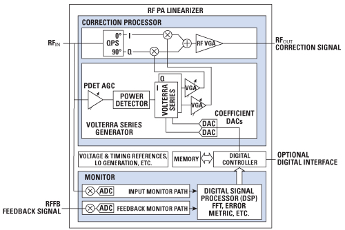
Figure 2 Pre-distortion integrated circuit block diagram.
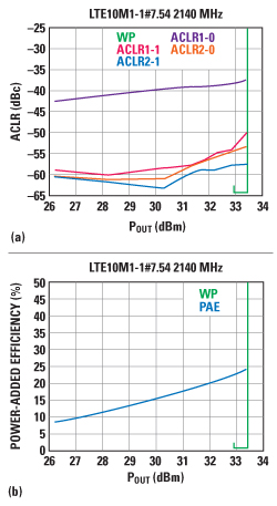
Figure 3 ACLR performance (a) and PAE performance (b) vs. power.
The pre-distortion solution is a fully-adaptive, RFin/RFout predistortion linearization solution that precisely compensates PA nonlinearities including AM/AM and AM/PM distortion, spectral regrowth, memory effects and other system level impairments (see Figure 2). It is optimized for Class A/AB and Doherty RF power amplifiers operating at an average power level of 500 mW to 10 W (rms). The module measures the feedback signal from the power amplifier output, and optimizes the correction function by minimizing distortion. The correction function is based on a Volterra series with memory terms but uses a unique linearization architecture that shifts complex signal processing from the digital domain into the more computationally efficient analog RF domain thus allowing it to operate with very low power consumption.
By compensating for these system level impairments, the integrated circuit allows a PA to transmit higher power at higher efficiency while still maintaining or exceeding the required system ACLR or distortion requirements. It can typically enable an existing Class A/B PA to transmit at least 3 dB more than the same PA operating in backoff. Now assuming that two different Class A/B PAs are transmitting the same power, the PA linearized will benefit from a 30 to 50 percent reduction in power consumption compared to the PA operating in backoff depending on the PAR and BW of the signal. The power consumption improvement even includes the integrated circuit power consumption which can be configured to be as low as 400 mW. It is important to note that some PAs may never reach desired linearity regardless of the amount of backoff with which they are operated. This situation may be experienced more often with wide BW and/or high PAR waveforms.
Using an example PA (TriQuint AP561) operating in linear mode and transmitting a 7.54 dB PAR waveform typical of what can be experienced with an LTE signal, the PA would in theory have an maximum rms operating point of 31.46 dBm – still more than 1.5 dB less than the required 33 dBm needed at the output of the PA in order to achieve 30 dBm at the antenna. However, when the PA is optimized for peak power in conjunction with the pre-distortion integrated circuit, the performance of the entire transmit path is significantly improved. As can be seen in Figure 3, the pre-distortion provides 16 dB of correction easily enabling the PA to meet the −50 dBc linearity requirement at an operating point at nearly 33.5 dBm. Additionally, since the PA is able to operate at a much higher operating point, it is now able to achieve efficiency of greater than 24 percent.
This combination provides designers an innovative platform solution that may be brought to market very quickly using components available and in production today. With minor changes to the bill of material and no changes to the printed circuit board design, this solution can support all global cellular bands, 3G and 4G protocols including WCDMA, LTE. The solution can also support other protocols as well as varying numbers of carriers adding up to a total signal BW of up to 20 MHz or less.