
Wavelength Division Multiplexing Passive Optical Networks (WDM PON) have recently been commercialized by vendors including LG, Nortel and Alcatel-Lucent, and are considered by many to be higher performance than Time Division Multiplexing (TDM) PON systems, which are widely deployed today. Adding broadcast service to TDM PON is relatively simple, as it requires the addition of a single downstream wavelength. For WDM PON, it is more complex, since the 1:N Arrayed Waveguide Grating (AWG) used at the remote node requires a broadband light source to broadcast to N users. AT&T Labs Research and Development in Middletown, NJ, has investigated the possibility of overlaying video and Gigabit Ethernet (GbE) through the direct modulation of a super luminescent light emitting diode (SLED), that acts as a broadband source (similar to an LED) with high power (similar to a laser source), which when coupled with an optical bandpass filter to eliminate wavelength interference with other channels, can excite the wavelengths of a 1:32 AWG. A high level block diagram of their proposed system, from central office to user, is shown in Figure 1.
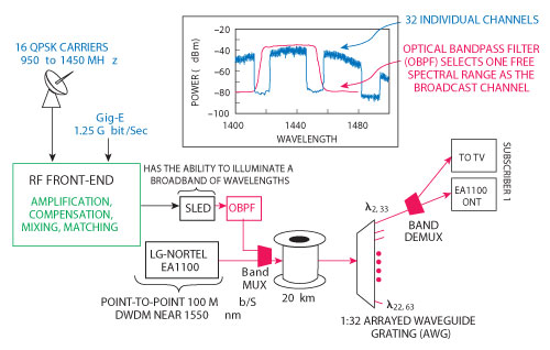
Figure 1 Broadcast service addition to a WDM PON network showing the necessary RF front-end circuitry before the SLED.
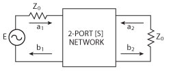
Figure 2 Two port network represented by its S-matrix.
One shortcoming of this technique is that the SLED has a poor modulation response. To this end, a small scale, passive gain equalizer implemented on a printed circuit board (PCB) was designed and measured, which shall be referred to as a compensator. Throughout this article, the simulations rely solely on AWR’s Microwave Office.
Compensator Design
In order to design the compensator, the electrical characteristics of the SLED are considered. By modeling it as a two-port network, as shown in Figure 2, the S-parameters can be measured to obtain its gain response. With a1 and a2 representing the incident waves and b1 and b2 representing the reflected waves on ports 1 and 2, respectively, S-parameter theory shows that
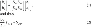
Figure 3 SLED |S21| magnitude (a) and phase (b).
which is a measure of the two-port network gain in a system that has input and output impedances matched to the characteristic impedance Z0 = 50 V.
The two-port S-parameters of SLED were measured using a vector network analyzer (VNA). A bias of 5 V and 142 mA was applied to the device through a bias tee to obtain the recommended operating conditions. The magnitude and phase response measurements of the SLED are shown in Figure 3. The gain response shows a 3 dB bandwidth of 340 MHz and over 30 dB loss in magnitude over the bandwidth of interest. The phase response has a linear regression correlation coefficient of roughly unity, corresponding to the almost constant group delay τg(f)≈35 ns of the SLED. With the responses shown, it was concluded that only the magnitude response of the SLED required alteration. Therefore, a passive compensator should, through attenuation at lower frequencies, emulate the following response:
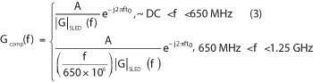
In Equation 3, A is a variable gain constant. The condition that the resultant response of the filter roll off exactly as a single pole lowpass filter after 650 MHz is an approximate specification – the results were deemed to be satisfactory as long as the overall response begins to consistently decrease in magnitude after reaching approximately 650 MHz at a rate of no greater than 50 dB/decade.
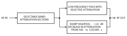
Figure 4 Block diagram showing the overall logic used in developing the compensator stage.
Given the necessity of obtaining sharp responses within the 650 to 850 MHz range, highpass characteristics were required. Simultaneously, in order to pass components at DC without the use of active circuitry, another parallel section was needed that was capable of providing the necessary low frequency attenuation, without completely blocking the signal within these ranges. Finally, frequency selective band-attenuation sections were needed at the onset of the circuit to gain additional control over the sharpness of the highpass response. Excluding the effects of loading between each stage, a block diagram of the network is shown in Figure 4.
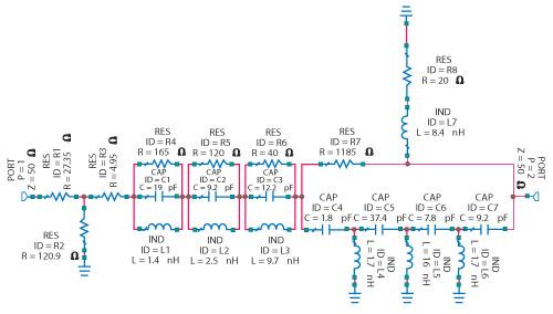
Figure 5 Compensator design using ideal circuit components.
Development of the necessary components in the circuit was accomplished using a seventh-order LC highpass filter, in parallel with a divider between a resistance and a resistance in series with an inductance. At the onset of the network, three RLC attenuation sections and a tee attenuator were placed for additional shaping of the highpass response. The resulting circuit, with ideal component values, is shown in Figure 5. The simulated response as compared to the ideal compensator response can be seen in Figure 6. There is less than 1 dB of difference between the ideal gain response and the response shown up to ~ 940 MHz. The response begins to deviate by greater than 1 dB after 960 MHz, with a maximum deviation of ~2.8 dB at 1.25 GHz.
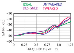
Figure 6 Comparison between the ideal, designed, untweaked, and tweaked compensator.
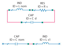
Figure 7 Inductor (a) and capacitor (b) models, factoring in fres and ESR.
Before fabricating the compensator, it was necessary to develop a sophisticated model of the circuit to determine possible variation in the output response. First, commercially available SMT inductors were chosen from Digi-Key Corp., since generally SMT inductors have less options and are more prone to self-resonance (fres) and equivalent series resistance (ESR) than SMT capacitors. The corresponding models used to simulate the effects of fres and ESR are shown in Figure 7. The calculations of Cd and Rs for the inductors employed the following equations:
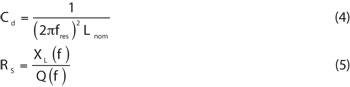
using the data provided in Table 1 for the chosen inductors. Similarly, Equation 4 can be rearranged to calculate Ls from Cnom.
From the quality factor (Q) data given graphically as function of frequency (not shown), it was determined that for each of the inductors chosen, the value of Rs would have insignificant effects on the compensator response above 100 MHz, since the reactance was at least eight times as large. Near DC, the value of Rs became so small that it provided an approximate short circuit relative to the generally large resistances surrounding the inductors. Even so, the inductor model in Figure 7 was implemented in Microwave Office, using a frequency-dependent resistance for Rs based upon the values of Q supplied by the manufacturer. The resultant circuit was simulated and plotted against the model with ideal component values (not shown). While the ESR and self-resonant characteristics were not seen to affect the designed response by more than a few dB, the inductor tolerances were seen to affect the compensator response by as much as 7 dB, as shown in Figure 8. Therefore, it was determined that measuring their actual values on a VNA was necessary in order to emulate the ideal response.
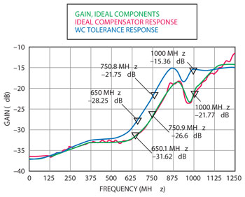
Figure 8 Response factoring the worst case tolerances on the inductors.
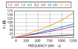
Figure 9 Measured inductance plots.
Once the inductors were received, they were soldered onto female flange SMA connectors, and their S11 characteristics were measured and displayed on a VNA’s Smith Chart. The resistive and reactive components of the inductors were measured as a function of frequency from 300 kHz to 1.25 GHz. The reactance plot is shown in Figure 9, and linear regression was run on the reactive data for each inductor, all of which gave a correlation coefficient of R2 ≥0.99, with the exception of the 15 nH which had R2 = 0.98. From the plots, the equivalent inductances can be calculated from
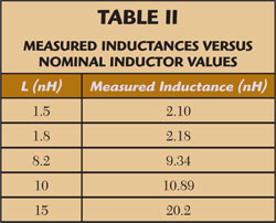
The values calculated from Equation 6 are shown in Table 2. It is important to note that despite the linearity of the reactance, each inductor is significantly larger than its nominal value.

Figure 10 Eagle board layout of the compensator.

Figure 11 Eagle board layout (a) fabricated compensator (b).
The measured inductance values were imported into Microwave Office, using the element ZFREQ, which allows for arbitrary definitions of resistance and reactance at specified frequencies and uses a linear interpolation model at all points between. At this point, it was necessary to retune much of the circuit, due to the non-idealities and deviation in nominal values of the inductors. To accomplish this, the compensator was cascaded with the SLED’s two-port model in Microwave Office and the real-time tuning feature was used to tweak the components of the circuit, while monitoring the resulting |S21|response. For instance, it was necessary to place an 8.2 nH nominal (measured 9.34 nH) in parallel with each of the 1.5 and 1.8 nH inductors in order to bring them closer to the specified values. C5 and L6 were noticed to have had little effect on the frequency response and were eliminated from the circuit. The updated compensator schematic is shown in Figure 10. The expectation is that the compensator will yield a passband ripple of less than 1 dB.
Compensator Fabrication and Testing
After completing the simulations, the compensator was fabricated and tested. Eagle was used to generate the necessary Gerber files for the etching of the board. The geometry used was coplanar waveguide (CPW) with ground. The substrate chosen was industry standard 62 mil-thick FR-4, which has little variation in its dielectric constant εr of 4.7 over the frequency range of interest and a loss tangent δ = 0.017. The copper signal traces used were 1 oz (1.4 mil), 35 mil wide with 7 mil isolation between the conductor and ground, guaranteeing approximately 50 Ω (50.6 exact) traces. Twelve mil diameter, round vias were placed around the components of the board (farther than 7 mil away). The input and output ports were reached through ~50 Ω traces extended to the edge of the board for side-mount SMA connectors. For convenience of shape, and to leave enough room for additional SMT components if needed, a 2" X 2" board was chosen. The routed Eagle board file and the fabricated compensator (built at Linearizer Technology in Hamilton, NJ) are shown in the top and bottom of Figure 11, respectively.
The measured compensator response, as compared to the designed and ideal responses, is shown in Figure 12. In the critical frequency range, from 0 to 650 MHz, the difference between the maximum and minimum deviations between the ideal and measured responses gives the passband ripple. This value was determined to be approximately 6.7 dB, taking the difference between the deviation at 250 MHz and at 650 MHz, which was ~4 dB higher than desired. In addition, although the flatness of the high frequency response is not as critical, the measurements were between 5 and 6 dB lower than the expected response of the compensator from 590 to 885 MHz. This will cause the overall system to have this amount of additional roll-off when operating within this frequency range.
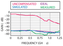
Figure 12 Comparison between the uncompensated, ideal, simulated and measured compensations responses.
Compensator Error Analysis and Tuning
As a result of the poor correlation between the designed and measured responses (which, even as is, would significantly improve the high frequency response of the SLED), the next step was taken to determine possible causes for the deviations. Feasible explanations are that incorrect component values were shipped, or that incorrect components were drawn from the packages when soldering. The sharp decrease in response from ~400 to 600 MHz is controlled by the value of C6 in Figure 9. Changing this value to 5.1 pF makes the measured and simulated responses agree over this band. At the highest frequencies, the value of C2 in the R2-L2-C2 band-attenuation section controls the sharpness of the response. Reducing this value to 5.1 pF makes the frequency responses from 1 to 1.25 GHz almost identical. In addition, the response drop that is expected to occur from 900 to 1010 MHz, a result of the R2-C2-L2 band-attenuation section, was not present in the measurements. This can be eliminated from the design by changing the value of R2 to 84.5 Ω (which is the nominal value of R1).
Another explanation for the lack of agreement between the responses is the tolerances on the component values. Most likely, at least some error was caused by deviation of the inductors from their nominal values, since the specific ones measured were seen to deviate largely, as shown in Table 2.
To correct the measured response, the compensator was tuned. Increasing C1 by adding a 2.7 pF capacitor in parallel had the desirable effect of bringing the frequency dip present from 950 to 1000 MHz in Figure 6 to a lower frequency range while simultaneously increasing its sharpness. R8 provided control over the low frequency attenuation, and therefore the ripple shown in this range was reduced by increasing its value to 39 Ω. The sharpness of the highpass response was improved by placing a 1 pF capacitor in parallel with C5. Finally, the reduction in the sharpness of the dip, now located at ~955 MHz, was accomplished by completely removing R3 from the circuit. The resulting response, as compared with the untweaked, designed, and ideal responses, is also shown in Figure 6. The difference between the maximum and minimum deviations, when comparing the tweaked and ideal responses, yields a ripple for frequencies below 650 MHz of only 2.75 dB.
Net Result
To observe the overall compensation, the measured two-port parameters of the compensator was imported into Microwave Office, placed in cascade with the SLED and the resultant |S21| response was measured. A graphical comparison of the uncompensated, ideal, simulated, and measured compensation is shown in Figure 12. It indicates that the 3 dB point of the SLED was increased from 340 to 550 MHz, and the overall response dip was decreased from over 30 dB to less than 12 dB, which constitutes significant improvement. It is also important to note that the phase response of the compensator had an insignificant slope as compared to the phase of the SLED, and thus the compensator preserves phase linearity. Even without the additional tuning, the compensator would have improved the SLED response significantly. Overall, the compensator shows a small-scale, cost-effective means of correcting for the poor modulation response of the SLED, which is of much utility when attempting to broadcast over WDM PON networks.
Chris Brinton is a first year PhD student at Princeton University, and received his BSEE (valedictorian and summa cum laude) in 2011 from The College of New Jersey. He holds various publications (current and pending) in the fields of power systems optimization, RF and microwave, fiber optics communications and digital signal processing. He has worked internships at AT&T Labs Research, Linearizer Technology and AT&T. His current research interests are in developing optimization algorithms to find and analyze minimum cost placements of renewable energy generators in congested electric transmission systems.