
This article proposes a new form of three-dimensional (3D) structure that can be easily constructed at a low cost. The proposed structure creates a set by combining a component attached layer-board using a frame-board as a spacer. Another element of the proposed structure stacks these sets to realize a tile structure similar to how a container house is built. Each set is connected through vertical interconnections by a solderless-method, using fuzz buttons. A tile structure active Transmit/Receive module is created, based on the proposed structure and is applied to an active phased array radar, operating in the 18 GHz frequency range. The fabricated module and its test results confirm that the proposed structure is cost efficient and easy to realize.
Present and future microwave products are gradually transitioning into more cost effective and smaller sized models. Reflecting this trend, microwave module structures are also changing from 2D to 3D structures. A 3D structure, from a design engineer’s perspective, has some issues concerning spatial restrictions around signal line routing or component placements. However, compared to a 2D structure, a 3D structure can be miniaturized and its weight reduced as the volume and weight of the module are reduced.1 A 3D structure also requires fewer components for constructing the module; thus, it can be cost effective.2 Therefore, the 3D structure is of interest for these reasons.
Studies on 3D structures have developed rapidly in the area of transmit/receive modules (T/R modules) used in radar systems. In particular, an active phased array radar is composed of hundreds or thousands of T/R modules. The weight, volume and cost of each T/R module become important parameters in determining overall performance of the radar. Active phased array radars used in missile or airborne systems especially have tighter physical restrictions; thus, T/R modules used in these types of radars are gradually changing from brick (2D) to tile (3D) structures.3

Figure 1 The proposed tile structure.
This article proposes a new tile structure that can be easily constructed at a low cost. This proposal also includes a vertical interconnection structure that is necessary for realizing the tile. The design and fabrication of a tile structure active T/R module that can be applied to active phased array radar is presented and, finally, the possibility of the proposed tile structure is validated.
The Proposed Tile Structure
The key points that determine the structure of the tile type modules can be summarized into two topics: how the stacking is arranged and how its vertical interconnections are realized. These points can be resolved through the proper choice of the spacer. The role of the spacer is to create room between the neighboring layer-boards within the tile structure, thereby protecting components attached on the layer-board. It also works as the medium for vertical interconnection. The spacer, therefore, is a critical factor for the tile structure. Previous studies showed that many issues of the stacking and vertical interconnection were resolved by the use of metallic spacers. Metallic spacers are particularly useful for securing ground levels for stacked boards. However, the signal line and ground plane have to be isolated in the spacer to create a vertical interconnection. In other words, a vertical interconnection is created by inserting a dielectric element into the spacer so that signal lines of the vertical interconnection are created within that dielectric element.4-6
This article proposes a new tile structure that uses a non-metallic spacer, which provides trades-offs for the pros and cons of using a metallic spacer. Unlike the spacers used in previous studies, this new tile structure uses a non-metallic spacer and creates a solderless vertical interconnection method using fuzz buttons. The non-metallic spacer was created using the same laminate used to fabricate the layer-boards, which makes it insensitive to external influences such as pressure or temperature. The proposed tile structure is shown in Figure 1.
The core of the proposed structure is the way that the frame-board, which is used as layer-board, is combined. As shown in Figure 2, the ground planes of both the layer-board and the frame-board are soldered with solder balls. Here, the layer-board is considered as the “Floor” while the frame-board is the “Wall.” Therefore, the structure’s “Floor-Wall set” (F-W SET) is obtained. The F-W SET is soldered between ground planes of both the layer-board and frame-board and can thus secure ground level related problems, arising from the use of a non-metallic spacer.

Figure 2 Floor-wall set.
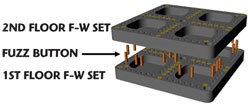
Figure 3 Stack of F-W sets using fuzz buttons.
The F-W SET stacking of the proposed tile structure is shown in Figure 3. This structure connects both the lower and upper F-W SET through vertical interconnections using fuzz buttons. The vertical interconnection that assembles each F-W SET is formed by a solderless-method. This allows users to conveniently repair, rework or replace the module, should any problem arise after module fabrication.

Figure 4 Structure of the proposed vertical interconnections.

Figure 5 Structure of the test fixture for the vertical interconnection.
Description of the Proposed Vertical Interconnection
Figure 6 Test-fixture for the vertical interconnection.
The proposed vertical interconnection uses the elasticity of the fuzz button to contact the neighboring layer-boards without soldering. This vertical interconnection structure is shown in Figure 4. The fuzz button is inserted into a signal via hole in the frame board so that the via hole and fuzz button together form a filled via. This signal filled via part and the neighboring layer-board’s signal line parts are in contact, thereby creating a vertical interconnection. The fuzz button, inserted into the frame-board, is contacted by pressure coming from the neighboring layer-boards.
The fuzz button used in the vertical interconnection is manufactured from a gold-plated nickel chromium alloy wire. It has a cylindrical shape with a diameter of 10 mils and a length of 70 mils and was manufactured by Custom Interconnects. The fuzz button has an insertion loss of approximately 0.5 dB and a return loss greater than 15 dB in the 18 GHz frequency range. For more convenient testing, the test fixture of the vertical interconnection consisted of two vertical interconnections and a transmission line that connected the two, as shown in Figure 5. The loss of the inserted transmission line is 0.03 dB/mm and the return loss is greater than 20 dB. The design goal of this test fixture was set based on the loss of the transmission line that connects the external connector and the vertical interconnection. Therefore, a single vertical interconnection was designed to generate less than 0.6 ± 0.05 dB of insertion loss and over 15 dB of return loss. This test fixture was designed to satisfy a 10 percent bandwidth at the center frequency. The simulation was done using HFSS V.11 from Ansoft.
A test fixture was created, using a RO3003 series laminate from ROGERS to fabricate the layer-board and frame-board. The thickness of the layer-board is 15 mils and that of frame-board is 60 mils. Super SMA series connectors (214-521SF) by Southwest Microwave were used as an external connector. Figure 6 shows the test fixture for vertical interconnection and Figure 7 shows how the fuzz button is inserted into the frame-board.
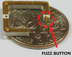
Figure 7 Fuzz button on the frame-board.

Figure 8 Characteristics of the test fixture for the vertical interconnection.
The fabricated test fixture was tested using a 8510C vector network analyzer from Agilent. Figure 8 shows the comparison of results from test fixture measurement and simulation. The test showed that the test fixture has an 11 percent bandwidth at a 17 to 18 GHz range and has an insertion loss of 1.6 dB and a return loss greater than 14 dB. By removing the characteristics of the 10 mm transmission line from the measured result, each vertical interconnection shows an insertion loss of approximately 0.65 dB. This test allowed us to confirm that the characteristics of the vertical interconnection satisfy the design goals.
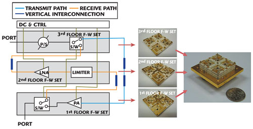
Figure 9 Proposed active transmit/receive module tile structure.
Design of the Proposed Active Transmit/Receive Module Tile Structure
Based on the proposed tile structure, an active T/R module was designed that can be applied to an 18 GHz frequency range. The proposed structure was validated by eliminating functional components such as the attenuator and driving amplifiers and the structure was simplified by only maintaining the key components needed for the T/R module. A hypothetical active phased array radar was considered and the specifications of the T/R module were calculated, using the radar equation so that it can be applied to the supposed radar system.7 The design specifications were set so that the transmit path would have more than 13 dB of gain, more than 10 dB of output return loss and an output power more than 26 dBm. The receive path was set to attain more than 8 dB gain, more than 10 dB input return loss and to satisfy a less than 8 dB noise figure. The simulation was performed using the HFSS V.11 from Ansoft and ADS 2008 from Agilent.
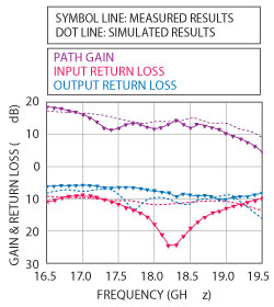
Figure 10 Characteristics of the transmit path (gain and return loss).
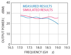
Figure 11 Characteristics of the transmit path (output power).
The active T/R module that was fabricated based on the proposed tile structure is shown in Figure 9. The proposed T/R module tile structure has a 2 × 2 array form; thus, it consists of four layer-boards and three frame-boards. One layer-board is a bias board which is positioned to transfer the T/R module’s DC bias and control bits from the outside. The proposed T/R module shown eliminates the bias board and thus consists of three floors of F-W SETs. Each of these three floors is structured as shown in the schematic diagram on the left of the figure. The first floor F-W SET is connected to the radiation element and is installed with a power amplifier in the transmit path and a switch that separates the transmit and receive paths. The second floor F-W SET is installed with a limiter and a low noise amplifier in the receive path. Lastly, the third floor F-W SET is installed with a switch that separates the transmit and receive paths and the phase shifter that is connected to the control circuit. Vertical interconnections between each floor were connected with a solderless-method, using fuzz buttons in the RF path, DC bias and control bits.
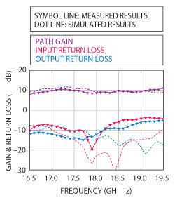
Figure 12 Characteristics of the receive path (gain and return loss).
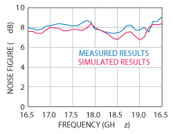
Figure 13 Noise figure of the receive path.
Figure 10 shows the gain characteristics of the transmit path, which was confirmed as 13±1.5 dB, as well as the return loss characteristics of the transmit path, which were confirmed as more than 10 dB as specified. Figure 11 shows the output power characteristics, confirmed to be over 25 dBm. Figure 12 shows the characteristics of the receive path, with a gain of approximately 9 dB and a return loss greater than 10 dB. Figure 13 shows the noise figure of the receive path, which is approximately 8 dB. The fabricated active T/R tile structure module resulted in characteristics that almost satisfied the design specifications.
The fluctuations of the test results are thought to be created by the possible occurrence of an imperfect ground between the stacked F-W SETs. The possible imperfect ground could be secured by a thin film gasket.8
This new tile structure, created by stacking the boards (F-W SET) through vertical interconnection using fuzz buttons, was built and tested. Some aspects require further resolution; however, the feasibility of the proposed structure was confirmed.
Conclusion
This article proposes a new type of tile structure that is unlike those proposed in previous studies and can be applied more conveniently and easily. The proposed tile structure was constructed using a spacer made out of the same laminate material used to make the layer-board. Creation of both the layer-board and frame-board from the same laminate material made the F-W SET less sensitive to external influences than when they are formed using different materials. This article also shows a solderless method to realize the vertical interconnecting using fuzz buttons. The module was constructed by stacking F-W SETs using the solderless-method so that any identified problems after fabrication could be easily fixed. The proposed tile structure is more cost-effective and easier to fabricate, compared to other structures proposed in previous studies. Therefore, the proposed tile structure can be easily duplicated by other engineers and other tile structures with better performances can be realized through further studies.
Acknowledgment
This research was supported by the Agency for Defense Development Korea, through the Radiowave Detection Research Center at Korea Advanced Institute of Science & Technology.
References
- M.S. Hauhe and J.J. Wooldridge, “High Density Packaging of X-Band Active Array Modules,” IEEE Transactions on Components, Packaging and Manufacturing Technology – Part B, Vol. 20, No. 3, August 1997, pp. 279-291.
- J.J. Wooldridge, “High Density Microwave Packaging for T/R Modules,” 2005 IEEE MTT-S International Microwave Symposium Digest, Vol. 1, pp. 181-184.
- K. Axelsson, “Generic Packaging Technologies for T/R-modules,” 2005 European Microwave Conference Digest, Vol. 2.
- J.J. Wooldridge, “High Density Interconnect (HDI) Packaging for Microwave and Millimeter Wave Circuits,” 1998 IEEE Aerospace Conference Proceedings, Vol. 1, pp. 369-376.
- T. Barbier, F. Mazel, B. Reig and P. Monfraix, “A 3D Wideband Package Solution Using MCM-D BCB Technology for Tile TR Module,” 2005 13thEuropean GaAs and Other Semiconductors Applications Symposium Digest, pp. 549-552.
- Y. Mancuso, “Thales Components and Technologies for T/R Modules,” 2008 IEEE Radar Conference Digest, pp. 1-5.
- M.I. Skolnik, “Introduction to RADAR Systems,” Third Edition, McGraw-Hill, New York, NY, 2001, pp. 30-97.
- TECKNIT Homepage, www.tecknit.com.