
Bandpass filters are employed in numerous microwave applications such as communication systems, radar and test equipment. Microstrip edge coupled structures are often used for bandpass filters because they are relatively easy to implement in printed circuit board (PCB) technology. These filters have many advantages, however, they suffer from an inherent issue with harmonic spurious responses. There are many techniques to address the suppression of these responses, however, each have their own concerns. The harmonic suppression procedure outlined in this article has minimal impact on design complexity and has some additional benefits for the microstrip PCB features, which are often in addition to the filter pattern on some designs. The design process will be outlined, models defined and circuit performance will verify the procedure.
The center bandpass frequency (f0) of a microstrip edge coupled filter will have spurious responses at even harmonic frequencies, that is unwanted filter responses at 2f0, 4f0, 6f0, etc. Specifically, the band at 2f0 has a detrimental effect on symmetry of the intended passband and can impact the bandwidth. The spurious responses occur because the phase velocities of the even and odd mode for each filter element are different.
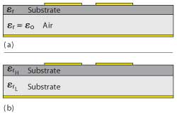
Figure 1 Cross-sectional views of a suspended coupled microstrip (a), and a composite laminate coupled microstrip (b).
There are many methods to suppress the 2f0 mode and most of these methods attempt to equalize the phase velocity of the even and odd modes. The use of over-coupling1,2 is done to extend the phase length of the odd mode to equal the even mode phase velocity. Another method3,4 uses capacitors to extend the travel path of the odd mode. A sawtooth pattern or wiggly coupled5 segment is used to lengthen the odd mode path, while maintaining a relatively unchanged even mode path and equalizing the phase velocities. Additionally, suspended microstrip configurations have been employed6 to equalize the modal phase velocities. All of these methods introduce their own set of capabilities and limits, however, in general, increase the design cycle difficulty. In the case of the suspended microstrip, shown in Figure 1, the design cycle is less impacted, but achieving proper dimensional control in the circuitry with effective multilayer via hole interconnections can be extremely challenging.
The current work offers a variation on suspended microstrip and utilizes a composite substrate copper clad laminate. The laminate uses two dielectric layers, which have significantly different relative permittivity (εr). As opposed to the suspended microstrip, this composite laminate concept can be processed through normal PCB fabrication processes, have plated through hole vias and are assembled like most other PCBs.
Composite Laminate Definition
The copper clad laminate used to fabricate the microstrip circuitry should ideally be the same type of substrate, however, with very different εr. Several variations have been evaluated, but only a composite laminate substrate, using layers of RO3010™ and RO3003™ materials, will be discussed here. The choice of these materials is due to their proven ability to be used in a variety of high volume and multifaceted PCB configurations. Additionally, these materials are from the same substrate family, so there are no concerns for material compatibility issues. The RO3010 material has a suggested Design Dk (εr) of 11.2 and the RO3003 substrate has a suggested Design Dk of 3.0. This difference in εr is enough to alter the odd mode phase velocity to approach an equalization of the even mode.
The composite laminate uses the dielectric layer with the high εr adjacent to the signal plane and the low εr material next to the ground plane as shown in the figure. There is a ratio consideration for the thickness of the different εr materials to be used in the composite laminate. A comprehensive study for even-odd mode equalization regarding edge coupled microstrip structures7 suggests some general design rules for frequencies below 20 GHz. When using layered dielectrics with εr ratio of 3.5:1 to 4.5:1, the thickness ratio should be 2:1, with the thicker substrate being the high εr material and placed against the signal plane. Recent experiments have shown that the high εr material can be thinner than the low εr material and still have benefits regarding altering the odd mode phase velocity. Even though this configuration is not optimum for a near perfect equalization of the odd and even mode phase velocities, it does have enough effect on the odd mode velocity to help minimize the 2f0 response.
Having the composite laminate with a thin layer of the high εr material and a larger thickness of the low εr material is beneficial for achieving a composite z-axis (thickness) εr value that is closer to the low εr material value. For microwave features that predominately use the z-axis εr properties of this laminate, such as transmission lines, this enables wider conductor widths for less conductor losses. Essentially a composite laminate can be constructed, which will give a nearly equal even-odd mode phase velocity for suppressing the 2f0 mode, have a high εr value near the signal layer to give improved bandpass performance of coupled features and have a lower z-axis εr in order to maintain wider conductor widths which will yield less conductor loss.
Even and Odd Mode Operation for Edge Coupled Microstrip Features
For a microstrip edge coupled feature, the even and odd mode phase velocity can be approximated by:8
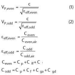
where VP is the phase velocity for either even or odd mode, εeff is the effective dielectric constant for even or odd mode and C is the various capacitances. Ceven, air is the capacitance of the microstrip structure when air is used as the substrate for the even mode and the same nomenclature applies to the odd mode. Cp is the parallel plate capacitance, Cf is the fringing capacitance, Cf' is the fringing capacitance in the even mode only at the magnetic wall, Cga is the gap capacitance due to coupling in air, Cgd is the gap capacitance in the dielectric and c is the speed of light in free space. Figure 2 gives a visual depiction of the even-odd mode operation of coupled microstrip features.
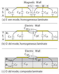
Figure 2 Cross-sectional view of a microstrip edge-coupled filter element.
When considering the even mode operation, it can be seen that the phase velocity will be affected by the dielectric properties of the laminate only. The odd mode phase velocity associated with the quasi TEM wave propagation is affected by the laminate as well as the capacitive gap coupling in the air (Cga). The odd mode phase velocity will be faster than the even mode just by the nature of using air in the gap coupling. The composite laminate can slow the odd mode phase velocity by the use of a thin layer of high εr substrate. The capacitive gap coupling (Cgd) using the high εr material, in combination with the capacitance gap coupling (Cga) in the air can be made to approximate the phase velocity of the even mode.
Outline of Filter Design Procedure
Several different edge coupled filters were designed in order to evaluate different composite laminate configurations. Furthermore, filters were designed at different frequencies and bandwidths to evaluate the effects of coupling as well as E field depth penetration into the higher εr material.
The filter design, which will be discussed in more detail, is a 5 element (n = 5), Chebychev filter with a passband ripple of less than 0.5 dB, a fractional bandwidth of 0.07 and designed for a center frequency of 2 GHz. The procedure for defining the circuit features is a common ladder circuit, lowpass prototype method defined in many microwave texts.9,10 The n = 5 prototype parameters for this filter are:
g0 = g6 = 1.0
g1 = g5 = 1.7058
g2 = g4 = 1.2296
g3 = 2.5408
The design equations are given by:
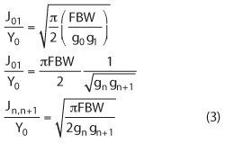
g0, g1…gn are the elements of the ladder-type low pass prototype with a normalized center frequency equal to 1. FBW is the fractional bandwidth of the filter. Jn, n+1 are admittances for the J-inverters and Y0 is the characteristic admittance of the terminating lines.
The desired even and odd mode impedances of each element of the filter are determined by:
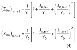
Once the even and odd mode impedances for each element are defined, the circuit pattern dimensions are determined by the use of a free software from Rogers Corp., MWI-2010. This software11 uses closed form equations to determine the even and odd mode impedance with a given circuit geometry and material properties. The software will also give the wavelength and for each element, the length of the element will be ¼ the wavelength, minus the extension due to fringing. Another method for determining the length of each element is given by:12
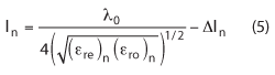
where εre is the even mode effective dielectric constant, εro is odd mode and Δln is the length extension due to field fringing. The MWI-2010 software can also calculate the length extension, using the well known closed form equations for microstrip configurations.13
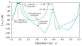
Figure 3 Comparison of simulated S21, using the same geometry with different substrates.
After the circuit dimensions are defined, a more thorough model is done, using the electromagnetic modeling (EM) software from Sonnet Software Inc. to fine tune the filter performance. Once the filter model is adequately defined on the composite laminate microstrip design, the model is repeated with a homogeneous laminate of the same composite εr . The results from these models are shown in Figure 3. The filter performance for the composite laminate is using a 0.127 mm (5 mil) layer of RO3010 substrate and 0.635 mm (25 mil) layer of RO3003 substrate, with the signal plane next to the RO3010 material. The homogeneous laminate is using a single substrate with a εr = 4.13.
It can be seen that the range of frequencies inthe 2f0 response region for the microstrip filter using the homogeneous substrate has an insertion loss of approximately –5 dB and the filter using a composite substrate has an insertion loss of –32 dB. Therefore, the spurious 2f0 response is significantly reduced with the use of the composite laminate. Furthermore, it can be seen that the bandwidth of the filter using the composite laminate is wider and the 2f0 response has a much narrower bandwidth, compared to the filter using the homogeneous laminate.
Measured Results
The composite laminate was made with the two substrates previously described, RO3010 and RO3003 materials. The homogeneous laminate used a TMM®4 copper clad laminate of the same thickness as the composite laminate. The choice of that material is based on the εr being near the desired value and the material being readily available.
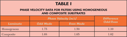
The information in Table 1 was found by using the MWI-2010 software for a microstrip edge coupled model, with an enhancement to include composite substrates. The phase velocity of the different segments of the filter was found and averaged. The physical PCB conductor layout for the filter is shown in Figure 4. The circuits were fabricated, assembled, tested and the measured results are shown in Figure 5. Tr2 is the S21 curve for the filter using a homogenous laminate and Tr4 is the S21 curve for the filter using the composite laminate. The markers were placed at two frequencies for each S21 curve. Marker 1 is the center frequency and marker 2 is the peak of the 2f0 response for the filter using the homogeneous laminate. Marker 2 has a |S21| peak of –7.3 dB. Marker 3 is the center frequency and marker 4 is the peak of the 2f0 response for the filter using the composite laminate, the peak of this 2f0 response is –31.3 dB. Although there are some differences from the measured results as compared to the model shown in Figure 3, the significant reduction of the spurious 2f0 response is verified.
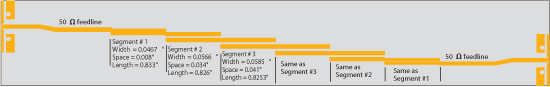
Figure 4 Physical PCB conductor layout of the microstrip filter.
The main difference of the measured results, as compared to the model, is a frequency shift. The composite laminate uses two substrates and the high εr substrate has a wider εr tolerance, which is typical of dielectric material with high εr values. The high εr material was within the manufacturers specification, however it had a slightly higher εr value than the nominal 11.2 given as the Design Dk. This accounted for the center frequency shift. The other frequency shift associated with the filter using the homogeneous material is a natural response of using the available TMM4 material, which had a slightly higher εr than the desired composite εr of 4.13. The TMM4 material has a Design Dk (er) of 4.5 and this too accounts for the frequency shift.
Other differences between the measured results and the model are attributed to the PCB manufacturing effects and tolerances regarding the circuit conductor patterns. These differences are likely the cause for the peaks of the 2f0 responses to be slightly different on the measured circuits as compared to the EM model.

Figure 5 PNA test results for the same circuit pattern using composite and homogeneous laminates.
Brief Overview of Extended Evaluations
Other circuits were modeled and evaluated with regards to the same material considerations. Some of the other issues evaluated were 3 element and 7 element filters, as compared to the 5 element filter shown previously. Intuitive assumptions were verified where less filter elements (3 element) had less benefit of the composite material for the 2f0 suppression. More filter elements (7 element) had a slight improvement over the 5 element results shown.
Additionally, there were alterations of the 5 element filter with changes in coupling, bandwidth and center frequency. Experiments were also performed using thinner composite materials, using a larger range of εr . These materials used the same high εr material (εr = 11.2) and the low εr material had an εr = 2.2. Due to the wide range of circuit patterns involved with the different filter elements and the material considerations, only general observations can be given here for the composite laminate:
- Tightly coupled elements will have more benefit than loosely coupled.
- Higher frequency filters can use a composite laminate with a thinner layer of the high εr material.
- Wider bandwidth can be achieved when using a larger ratio of εr values.
- As the laminate gets thinner, firm definition on the ratio of the high/low εr material becomes more critical.
The composite laminate procedure shown here can be very successful to minimize the spurious 2f0 responses, however thorough EM modeling is highly recommended. The filter models shown here demonstrated the concepts, but they were not optimized.
Conclusion
It has been shown that a composite laminate using the proper ratio of high/low εr material can significantly reduce the spurious 2f0 harmonic response of a microstrip edge coupled bandpass filter. It was also illustrated that the composite laminate can achieve wider bandwidth. In comparison to the many other techniques for reducing the 2f0 harmonic response, the composite laminate does not increase the design complexity and is capable of most common PCB configurations.
Additionally, there are other benefits to this technology, since many microwave PCB designs with filter features also have many other microwave structures. The added benefit of the composite laminate shown here is when the thinnest effective high εr material is used to reduce the 2f0 response, the overall z-axis εr value remains relatively low and this allows the other PCB features to have wider conductors. The wider conductors will allow other microwave features to have less conductor loss as well as improved PCB fabrication yields.
The composite laminate allows the designers to easily and significantly reduce the 2f0 harmonic response, increase the bandwidth and still maintain a lower z-axis εr value to allow other features on the microwave PCB to have lower losses.
References
- A. Riddle, “High Performance Parallel Coupled Microstrip Filters,” 1998 IEEE MTT-S International Microwave Symposium Digest, pp. 427-430.
- J.T. Kuo, S.P. Chen and M. Jiang, “Parallel-coupled Microstrip Filters with Over-coupled End Stages for Suppression of Spurious Responses,” IEEE Microwave and Wireless Components Letters, Vol. 13, No. 10, October 2003, pp. 440-442.
- S.L. March, “Phase Velocity Compensation in Parallel-coupled Microstrip,” 1982 IEEE MTT-S International Microwave Symposium Digest, pp. 410-412.
- I.J. Bahl, “Capacitively Compensated High Performance Parallel Coupled Microstrip Filters,” 1989 IEEE MTT-S International Microwave Symposium Digest, pp. 679-682.
- M.W. Zhou, L. Li, and Q.Y. Yin, “Optimal Model for Wiggly Coupled Microstrips in Directional Coupler and Schiffman Phase Shifter,” PIERS Online, Vol. 3, No. 2, 2007, pp. 32-135.
- J.T. Kuo, M. Jiang and H.J. Chang, “Parallel-coupled Microstrip Filter Design on Suspended Substrates for Suppression of Spurious Resonances,” IEEE Transactions on Microwave Theory and Techniques, Vol. 52, No. 1, January 2004, pp. 83-89.
- J.P. Gilb and C.A. Balanis, “Pulse Distortion on Multilayer Coupled Microstrip Lines,” IEEE Transactions on Microwave Theory and Techniques, Vol. 37, No. 10, October 1989, pp. 1620-1628.
- R. Garg and I.J. Bahl, “Characteristics of Coupled Microstriplines,” IEEE Transactions on Microwave Theory and Techniques, Vol. 27, No. 7, July 1980, pp. 272. Corrections IEEE Transactions on Microwave Theory and Techniques, Vol. 28, No. 3, March 1980, pp. 272.
- D.M. Pozar, Microwave Engineering, John Wiley & Sons Inc., Somerset, NJ, 2005, pp. 392-437.
- G. Mattaei, L. Young and E.M.T. Jones, Microwave Filters, Impedance-Matching Networks and Coupling Structures, Artech House, Norwood, MA, 1980.
- B.C. Wadell, Transmission Line Design Handbook, Artech House, Norwood, MA, 1991, pp. 199-207.
- J.S. Hong and M.J. Lancaster, Microstrip Filters for RF/Microwave Applications, John Wiley & Sons Inc., Somerset, NJ, 2001.
- E. Hammerstad and O. Jenson, “Accurate Models for Microstrip Computer Aided Design,” 1980 IEEE MTT-S International Microwave Symposium Digest, pp. 407-409.