
Micro-electromechanical systems (MEMS)-based products run from the mundane of automobile air-bag sensors to the over-hyped optical switching fabrics of the recent telecommunications bubble. For some time now, design engineers have been waiting for the advantages of MEMS fabrication techniques to be successfully applied to the problem of RF and low current switching. The concept of using semiconductor fabrication processes to build devices with moving structures intuitively suggests that a MEMS-based device will deliver the high performance switching capability of an electromechanical relay with the speed, size and cost of a solid-state FET or PIN diode.
To date the majority of entrants into the MEMS relay field utilize some variation of electrostatic actuation where an electrical charge is used to draw contact points together in order to complete a circuit. While many pursue variations on the electrostatic MEMS theme, Magfusion Inc. is taking a decidedly different approach. The company has developed a switch technology that uses magnetic fields to assist in both switch actuation and no-power latching. Recently, the company introduced MagLatch, the first RF relay that utilizes this new approach to switching.
MEMS is viewed as a natural solution for mechanical RF and low power switch applications due to the promise of improvements in size, cost and performance. Thousands of MEMS switches can be batch fabricated on a single silicon wafer (see Figure 1) using standard integrated circuit production methods. The resulting switches routinely demonstrate RF performance to 20 GHz and beyond because the parasitics associated with these microscopic devices are extremely small. While the size and performance benefits of MEMS are well known, the technology has proven to be deceptively difficult to commercialize. To date, only a few MEMS switch products have been made commercially available despite several years of development efforts. This suggests that the electrostatic actuation approach has several inherent technical challenges. Magfusion's alternative magnetic approach has traditionally received much less attention, but avoids many of the previously encountered difficulties.
| |||||||

Some of the basic characteristics of the MagLatch RF MEMS switch are summarized in Table 1. The device is a magnetically actuated DC to 6 GHz SPDT latching switch in a hermetic package. The theoretical switching speed of the device is approximately 5 kHz, but for most practical applications, this capability is not required. As a direct consequence of using magnetic actuation, the set and reset voltages are less than 5 V, which is unusually low for a MEMS switch. Because the device so closely parallels traditional mechanical relay architecture, the magnetic MEMS switch delivers exceptional RF performance, low insertion loss, and high isolation and linearity. The values listed in the table are actually limited by the package and not the switch itself. Contact life is rated at 1 million cycles for a bias condition of 10 V and 10 mA and 10 million cycles with no load applied to the contacts during switching.

MagLatch MEMS Switch Structure
The basic structure of the MagLatch micro switch is illustrated in Figure 2, which depicts a simplified switch die in a SPST configuration (initial MagLatch products are SPDT devices). The movable switching element is a soft magnetic cantilever structure composed of Ni80Fe20 alloy (permalloy) supported at its center by a torsion hinge. The cantilever is raised above the surface of the die about 10 mm, such that it is able to rotate about the torsion hinges. The size of the cantilever is roughly 0.5 x 0.5 mm. A movable top contact is located at one (single pole, single throw or SPST) or both (single pole, double throw or SPDT) ends of the cantilever. In order to optimize the RF performance of the device, the contact tip is electrically isolated from the bulk of the cantilever using an intermediating dielectric region. The RF signal propagates through the switch on a microstrip transmission line, which also forms the bottom fixed contacts. The transmission line conductor contains an open gap directly beneath the top contacts. When the cantilever is in the up position, the incident RF signal is reflected by the open gap so the switch is in the off position. When the cantilever is in the down position, the top contacts electrically shunt the gap by making a metal-to-metal contact turning to the on position. A small permanent magnet is attached either above or below the cantilever. This magnet is polarized so that the magnetic flux lines are vertically oriented, perpendicular to the plane of the cantilever. That is to say, the magnet's north and south poles correspond to the flat circular faces. The permanent magnet is used to latch the cantilever in the on or off position, and consequently provides the contact force. A planar spiral coil is situated under the cantilever such that half the coil is beneath the cantilever. The coil is used to electrically toggle the cantilever from one latched state to the other as will be explained in more detail below. It can be noted from Figure 2 that the control signals that pass through the planar coil are totally separate from the RF signal path, which is confined to the microstrip lines and the cantilever contact tip. The switches are fabricated on silicon wafers using conventional planar processing methods, with the exception of the NiFe cantilever, which is deposited using an electroplating process. The overall dimensions of a SPDT die including bond pads are approximately 1.7 x 2 mm.
| |||||||

Principles of Operation
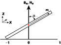
Having described the physical components that make up a magnetic latching MEMS switch, one can fast forward to the basic operating principle. To start, consideration should be given to how the magnetic latching operation is accomplished. When the length L of a permalloy cantilever is much larger than its thickness t and width w, the direction along its long axis becomes the preferred direction for magnetization otherwise known as the easy axis. When the cantilever is placed in a uniform magnetic field (in this case, produced by the underlying permanent magnet), a magnetic torque is exerted on the beam that will attempt to rotate the cantilever until it is aligned with the external magnetic field. The direction of the rotation can be in either direction (cw or ccw) and is determined by the position of the cantilever relative to the magnetic field — the magnetic torque will favor the direction that minimizes the rotation angle. This bi-directional rotation, illustrated in Figure 3, produces two stable states for the cantilever that are held by magnetic forces. This magnetic bi-stability is the enabling mechanism that produces a magnetic, no-power required, latching MEMS switch. It is important to note that the actuation force on the cantilever is bi-directional, alleviating the need for a mechanical return spring. To aid in a physical understanding of bi-stability and the parameters that affect the magnetic MEMS switch operation an analytical expression for the magnetic force as a function of cantilever angle is in order.
| |||||||
Electrical Switching
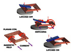
The device is toggled from one state to the other by passing a short current pulse through the switching coil. In general, when current flows in a coil, a magnetic file is produced that circulates around the coil in a direction described by the "right hand rule." Recall from the diagram that only half of the coil is situated under the cantilever and, because of this geometry, the field produced by the switching coil is directed horizontally along the length of the cantilever. To switch the device, the magnetic field produced by the switching coil momentarily reverses the direction of the magnetization m and causes the device to toggle (governed by ![]() m = m x B0). These concepts are summarized in Figure 4, which shows the initial latched state, the magnetic fields that interact to switch the device and the final latched state. A current pulse through a planar spiral coil produces a circulating magnetic field. The direction of the circulating magnetic field depends on the direction of current flow. The red arrows represent the magnetic field produced by the flow of current, represented by the purple arrows. The top figure shows the initial magnetically latched state of the switch. The middle figure shows how the magnetic fields from the coil momentarily oppose the magnetization vector in the cantilever and cause the device to toggle, and the bottom figure shows the final latched state of the device. Note that since the ON and OFF position of the cantilever are held using magnetic fields, the switch consumes zero power in these states.
m = m x B0). These concepts are summarized in Figure 4, which shows the initial latched state, the magnetic fields that interact to switch the device and the final latched state. A current pulse through a planar spiral coil produces a circulating magnetic field. The direction of the circulating magnetic field depends on the direction of current flow. The red arrows represent the magnetic field produced by the flow of current, represented by the purple arrows. The top figure shows the initial magnetically latched state of the switch. The middle figure shows how the magnetic fields from the coil momentarily oppose the magnetization vector in the cantilever and cause the device to toggle, and the bottom figure shows the final latched state of the device. Note that since the ON and OFF position of the cantilever are held using magnetic fields, the switch consumes zero power in these states.
| |||||||
Electrical Characteristics
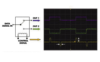
The AC switching characteristic of an SPDT RF switch is shown in Figure 5, which includes a schematic diagram of the switch and measured data from an oscilloscope. The bottom trace on the right shows the control signal connected to the switching coil, which consists of ±5 V (60 mA), 100 µsec pulses. The two upper traces on the right are the switched data signals through the device. It can be seen that the device is switched on the leading edge of the control signal and remains latched in that state until the next switching pulse toggles the cantilever to the opposite side. Because the cantilever is latched using magnetic forces, the device requires zero stand-by power to hold a latched state. This feature also provides fault tollerance, since the switch will maintain its last valid state should the system lose power.
| |||||||
High frequency S-parameter data of a typical packaged MEMS switch is plotted in Figure 6, which presents insertion loss, isolation and return loss from DC to 10 GHz. The packaged device was probed directly on the solder bumps using coplanar RF probes having a pitch spacing equal to the package solder ball spacing. At 6 GHz, the insertion loss is seen to be approximately 0.4 dB, isolation is about 45 dB and return loss is approximately 20 dB. By way of comparison, a typical GaAs SPDT RF switch at 6 GHz will have an insertion loss around 1.5 dB, isolation of about 20 dB and a return loss of approximately 10 dB.
| |||||||

MEMS Package Design
Because the MEMS die has vulnerable micromachined structures exposed on the surface, special considerations must be made in the package design and the back-end assembly process. These challenges include pick-and-place manipulators that handle the die from the edges and package designs that incorporate a sealed cavity while providing good RF performance. Early MEMS development work tended to focus rather narrowly on the intrinsic (bare die) switch and either settle for very expensive package designs or, more typically, overlook the back-end process altogether. Conventional wisdom normally dictates that 70 to 80 percent of the total cost of a MEMS device is associated with the package and final test. Recent efforts by Microlab and others to commercialize MEMS devices have resulted in more cost-effective package methods.
| |||||||

The package design adopted by Microlab for the first generation of RF MEMS switches is shown in Figure 7. The 5 x 5 mm package is a hermetic type that consists of two alumina parts. A substrate that forms the bottom contains CuW vertical feed-throughs to the package bottom side and a lid containing an internal cavity. The MEMS die is attached to the top side of the substrate and wirebonded to internal pads. The lid is sealed using an AuSn alloy to prevent organic contamination. The external magnet is attached to the top exterior surface. MagLatch products are now in full production with immediate availability. For more information, visit www.magfusion.com.
Magfusion Inc.,
Chandler, AZ (480) 926-9500.
Circle No. 301