
A successful power amplifier (PA) design requires an assortment of design tools. Small-signal S-parameters will provide a measure of small signal stability, power gain and the required input and output termination networks to provide a conjugate matched network. These techniques are well suited to device operation in the small signal regime. However, large output power requirements subject the device to operation over a greater range of voltage and current and thus additional measures are required. Further parameters entering the design space include power, efficiency, linearity, harmonic distortion and thermal considerations and their effect on device reliability. These added factors call upon the nonlinear aspects of active load pull1 and polyharmonic distortion2 for the measurement and modeling process and device modeling applied to harmonic balance3 in simulation. However, in all cases, the resulting output of these collective efforts is a set of active device input and output terminations, Zs and ZL, provided by input and output matching networks (IMN, OMN). These matching sections satisfy performance criteria while permitting a large power device to conveniently operate in the system impedance. In addition, the networks provide for bias of the active device and collectively form a set of bias tees. The in-situ measurement process of active load pull places the device into large signal operation, stressing both the device thermal and electrical properties. An important first step in PA design is the characterization of a device performance as a function of termination impedance. Active load pull conducted first at small signal input levels provide device information analogous to S-parameter data collection.
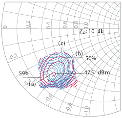
Fig. 1 Trade-off between power and efficiency for a given termination impedance at 2.2 GHz.
The Load Pull System and Procedure
Small-signal S-parameter data collection should precede load pull operation. The device stability and regions of potentially unstable terminations need to be assessed. This cannot be over stressed as power devices, which are permitted to enter uncontrolled oscillation, can be destroyed, leading to erroneous data and damaged test sets. Adding either series or shunt resistive losses to the input or output of the test set will stabilize the active device. Finally,
S-parameters will guide the selection of appropriate input and output load pull impedance regions for power gain.
In large power transistors, the goal is to find the appropriate real and imaginary terminating impedances at the device input and output, which maximize the device output power commensurate with minimum distortion and the deleterious effect of device heating. These terminating impedances are frequency dependent and must be obtained at multiple frequencies in order to map out an impedance trajectory vs. frequency.
The power gain, output power and drain efficiency are parameters provided by the load pull contours. Contours mapping of equal values are useful; however, their dependence and trade-off is not clear. Instead, a combined relationship between the parameter sets that provides a single concise objective is sought. Such a relationship was outlined previously;4 however, the approach to generate the contours was based on a simplified model of the intrinsic power device and did not target directly the approach taken in this work: temperature.
Combination Search Parameters Facilitate Load Pull Termination Selection
Fig. 2 Infrared camera used to characterize the temperature rise of a package device.
Historically, the output power, drain efficiency and power gain are the three main device parameters provided by the load pull contours. The impedance contours provided by these parameters are useful in themselves; however, it is not necessarily a straightforward process to determine how to trade off these parameters to achieve maximum device performance. Typically a sector line (a) is drawn (see Figure 1) to establish a tradeoff between the output power (b) and the efficiency (c). To address this challenge, the use of a combined relationship between these parameters that provide an additional concise design objective via the dissipated power contours is explored.
Increased operating voltage and the ability to dissipate tremendous amounts of DC power creates an increased concern for device reliability and robustness. A reliable power amplifier design is highly dependent on controlling the output power commensurate with the device junction temperature. For example, an Arrhenius plot for GaN-on-Silicon leads to a MTTF, which improves approximately ten-fold for each 20°C reduction in junction temperature.5 Therefore any reduction in junction temperature can have a significant impact upon device reliability.
The junction temperature, TJ, is dependent on the thermal resistance, device drain efficiency, power output and power gain. In addition, the materials and methods of attaching the transistor to the package affect TJ as well as these items being accounted for in the device thermal impedance, Rth. Tying these four parameters together leads to a temperature contour, which reveals the termination minimizing TJfor a specific power output. Determination of the device thermal impedance is the initial key to creating temperature contours. These contours are subsequently mapped against the device termination impedance. The thermal characterization is provided by an infrared (IR) camera, shown in Figure 2. Cooling the camera system is required for its operation and maintaining high optical sensitivity. The clear difference in device temperature profile and thermal impedance influenced by the packaging are shown in the IR camera image of Figure 3. The larger difference in device temperature rise between the two packages is noted in the white spot nearest to the drain terminal of the device b.
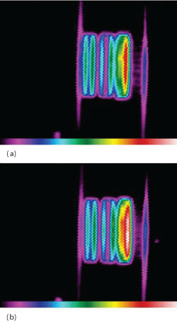
Fig. 3 Temperature rise for a copper-moly-copper (a) and copper-tungsten (b) package.
Conservation of energy dictates that the total power into the active device, the RF and the DC input power sum to the total power output, the RF power and the power lost as heat or the dissipative power. Therefore,

Equation 1 can be rewritten, recognizing that the power gain Gpand the DC-to-RF drain efficiency η are implicit. The power dissipation of the transistor is given by
The junction temperature is related to the product of the dissipated power and the device thermal resistance,
The parameter T0is the base plate temperature. Facilitating these calculations is accomplished if Equation 3 is recast in terms of the power added efficiency (PAE). Using Equation 2 and consolidating the power gain and drain efficiency gives

The load pull data collection provides contours of drain efficiency, output power and power gain vs. impedance. Once the thermal resistance is determined, typically with an IR thermal camera, the temperature rise of the device junction can be calculated.
Using Equations 2 and 3, the junction temperature rise and the resulting thermal contours are calculated, resulting in a fourth parameter being available to select optimum device impedances. The objective in using the thermal contours is to select impedance regions where the desired power, gain and drain efficiency coexist and then focus on the region that provides minimum rise in junction temperature. This methodology will provide the designer with an impedance set that not only optimizes device RF performance, but also maximizes the device reliability. In some cases, the impact can be an order of magnitude increase in device lifetime.
In this work, the definition of optimum load impedance refers to the impedance that minimizes the rise in junction temperature while meeting the targeted output power. In Figure 1, a typical power output and drain efficiency were shown at 2.2 GHz for a 24 mm GaN-on-Si HFET6 with 40 µm gate pitch, while the profile of Tj for the same frequency is shown in Figure 4. In all cases, the base plate temperature, T0, is held constant at 25°C and the measured Rth is 1.8°C/W.
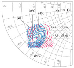
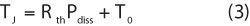
Fig. 4 Temperature open-contours (a) in 2°C increments and power output closed contours in 0.25 dB steps.
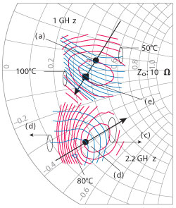
Fig. 5 Contours of constant temperature (open loci) and output power (closed contours) at 1 GHz (a) and 2.2 GHz (b).
The efficiency steps are 1 percent, while the temperature steps are 2°C. The range in drain efficiency spans 9 percentage points while the temperature spans a range of 30°C. The power contours consist of the peak power at 47.5 dBm and successive power steps, which are 0.25 dB below the peak. The ability to assess the appropriate load termination impedance, ZL, and its impact on junction temperature are shown in Figures 4 and 5. A lower TJ of 84°C occurs near the maximum drain efficiency ZL and has a real termination that is lower in value than for the peak power ZL. For example, the 47.25 dBm contour in Figure 4 shows a 30°C difference in TJ for the same output power.
Fig. 6 Constant output power region at 2.2 GHz display multiple temperature contours ranging from 80° to 135°C.
Application to Broadband Design
A temperature gradient vector points in the direction of increasing temperature and in effect consolidates drain efficiency, output power and power gain contours. At different frequencies, the angle of the vector will vary. This is illustrated in Figure 5, where the temperature gradients are shown to rotate in a counter-clockwise direction as the frequency changes from 1 to 2.2 GHz. The temperature and power steps are 5°C and 0.5 dB, respectively.
At 1 GHz, a decrease in the real impedance of the termination increases the temperature, while at 2.2 GHz the opposite occurs. For the same output power, there exists multiple impedance points, which provide differing temperature rise. For example, at 1 GHz, Figure 5 (a) is 25° cooler than Figure 5 (e). Broadband application of the amplifier and ease to impedance match requires thermal impedance points vs. frequency not too far apart and closest to the chart center. At 1 GHz, while higher output power is possible, it will be at the risk of higher TJ. In essence, the increase in power output is not complemented by a larger increase in drain efficiency. Furthermore, if the impedance points are constrained by the matching network, an increase in TJat lower frequency occurs, since these impedance points are not satisfied, see Figure 5 (e) vs. 5 (a). Clustering the impedance values to facilitate broadband matching requires the target impedance set to meet as (b) and (e) of Figure 5 and not (a). The resulting increase in temperature, TJ, at 1 GHz is evident. The optimal thermal drain impedances loci migrate in opposite directions; the lower frequency favoring higher real impedance, the higher frequency favoring lower.
The impact on the selection of terminations is particularly acute when investigating amplifier efficiency alone. It is instructive to look at a device at constant output power as seen in Figure 6 at 2.2 GHz and 47.5 dBm. At constant output power, the power gain is nearly constant and maximum drain efficiency correlates well with the minimum TJ. The value of TJ varies by over 55°C over this power output region. Therefore, the selection of ZL has a significant impact upon the TJ and hence device reliability. Unlike conventional load pull contours displaying a range of output power, when the output power is held constant, the contours of temperature align well with the contours of drain efficiency. Evidence of the junction temperature difference due to the selection of drain termination (see Figure 6a and b) is apparent in the drive up the curve at a single frequency of 2.2 GHz. Two selected termination impedances are chosen, one at low TJ (a) and one at high TJ (b). The resulting temperature rise vs. power output is shown in Figure 7. At (a) the termination at the device lead is 2.51-j3.72 Ω,while at (b) is 3.68-j5.05 Ω. The TJ difference is at least 30°C at moderate power output.
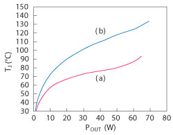
Fig. 7 Junction temperature rise as a function of output power for two selected drain impedances of 2.2 GHz.
This work is applicable to power amplifiers operating in the pulse mode. The temperature contours are simply linear scaled from parameters of efficiency, output power and thermal resistance. Although these elements will shift slightly in value from CW operation to pulse operation, the shift will be properly captured during active load pull. However, the value of thermal resistance from IR scans should be captured while the device is operating in the pulse mode and should be no different than the CW mode.
Circuit Implementation and Results
Application of the design method over a broadband begins with a collection of load pull data spanning 1.2 to 1.9 GHz. During load pull, the maximum power output is limited to 47.5 dBm, nearly 60 W. Measured and calculated load pull parameters and a measured Rth are subsequently used to generate optimal impedances at each frequency for a target TJ of 70°C. This constitutes a load impedance table. A source table is found by searching first for maximum Gp at each frequency and moving along the associated constant reactance contour, while aiming to increase the real part of the source. The effect of this approach improves linearity and furthers the ability to broadband the design of the input matching network.
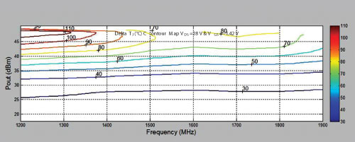
Fig. 8 Junction temperature rise assembled from measured drive up characteristics of the power amplifier.
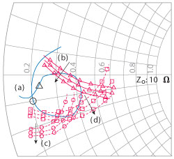
Fig. 9 Simulated drain port reflection coefficient obtained from measurements vs. frequency, 0.8 to 2.2 GHz (a), triangle point at 1.1 GHz, square at 1.7 GHz and circle at 1.9 GHz.
The impedance tables were used in the construction of a broadband amplifier circuit spanning a frequency range of 1.2 to 1.9 GHz. Measured results of Pout and TJ vs. frequency of the broadband board are shown in Figure 8. Measurement and co-simulation of the power amplifier drain port impedance via its reflection coefficient, Figure 9 (a), with the overlay of the temperature contours show good agreement with measurements of the completed amplifier, Figure 8. The amplifier reflection coefficient misses the targeted thermal contour at 900 MHz, is properly centered for 1.2 to 1.9 GHz operation and is off target beyond 1.9 GHz.
The measured amplifier OMN, shown in Figure 10 and the drain reflection coefficient require modeling and co-simulation with an electromagnetic simulation (EM) tool. The drain reflection coefficient measurement is facilitated by an SMA connector launch. However, there exists a substantial electrical difference, a 35.2 ps delay, between the connector launch and the power amplifier package lead. Validating card measurements requires VNA calibration. Then, the port extension is enabled in the VNA and used to account for the SMA delay during measurement. The measured card is modeled completely with both the discrete elements and EM simulation of the transmission lines. This EM simulation is completed using AXIEM.7 The edge port for launch for this initial simulation of the transmission lines on the card is the width of the SMA pin. Subsequently, after the model and the simulation of the card agree with measurement data, another EM simulation is required where the edge port launch is now the width of the package lead. The resulting final simulation is shown in Figure 9 (a).
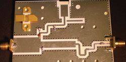
Fig. 10 Drain side bias line and termination or output matching network with SMA measurement launch on the left.
Conclusion
A PA design technique was presented, which focuses on control of device temperature rise by careful selection of the termination impedance. Thermal contours are assembled from conventional load pull data which is post processed. A measured 1.2 to 1.9 GHz, 60 W amplifier design demonstrates correlation with the method. Circuit measurement and simulation with validation requires co-simulation with EM and modeling of all discrete elements. The technique outlined in this work leads to a favorable selection of terminations which is less prone to error as the objective is concise.
Acknowledgment
The authors thank Michael Kendall for his extensive data collection and the post process measurements.
References
- I. Angelov, H. Zirath and N. Rorman, “A New Empirical Nonlinear Model for HEMT and MESFET Devices,” IEEE Transactions on Microwave Theory and Techniques, Vol. 40, No. 12, December 1992, pp. 2258-2266.
- J. Verspecht and D.E. Root, “Polyharmonic Distortion Modeling,” IEEE Microwave Magazine, Vol. 7, No. 3, June 2006, pp. 44-57.
- “Device Modeling with NVNAs and X-Parameters,” 2010 IEEE Workshop on Integrated Nonlinear Microwave and Millimeter-wave Circuits (INMMIC), pp. 12-15.
- B.W. Leake, “The Analytical Construction of Power-dissipation and Efficiency-contours from Load Pull Data,” 1983 IEEE ARFTG Conference Digest, Vol. 3, pp. 31-38.
- S. Singhal, T. Li, A. Chaudhari, A.W. Hanson, R. Therrien, J.W. Johnson, W. Nagy, J. Marquart, P. Rajagopal, J.C. Roberts, E.L, Piner, I.C. Kizilyalli and K.J. Linthicum, “Reliability of Large Periphery GaN-on-Si HFETs,” Microelectronics Reliability, Vol. 46, No. 8, August 2006, pp. 1247-1253.
- Nitronex Corp., NPT1014 Data sheet, www.nittronex.com
- Applied Wave Research, AXIEM, www.awrcorp.com
Alan Victor received his doctorate from North Carolina State University. He is a principal engineer with the Nitronex Corp., where his current interests are in the development of microwave power amplifiers and MMIC designs utilizing GaN-on-Silicon. Prior to joining Nitronex, Dr. Victor was with the IBM Microelectronics Group, Harris Microwave and the Motorola Communications Sector. He co-founded a wireless data communications company and has 10 issued patents and over 100 publications.
Walter Nagy has more than 25 years of microwave experience and is a principal engineer at Nitronex Corp. where he has worked since 2001. In his current role, Nagy is the RF technical lead on Nitronex’s 48 V GaN product line and supports advance technology development. He has experience with high power load pull measurements, nonlinear device modeling, device thermal simulations and device level robustness and reliability testing. Nagy’s prior role at Nitronex was in applications engineering where he developed evaluation boards and supported customers for wireless infrastructure and broadband military applications.