
By building a better electromagnetic (EM) simulation model, which includes the effects of a PCB’s metal surface roughness, microstrip and coplanar waveguide, circuits can be closely compared to find the best fit for different applications.
Matching a microwave transmission-line technology to an application requires careful consideration of more than a few factors. Depending on the requirements of an application, high-frequency circuit designers may be concerned with loss budgets, propagation mode issues, radiation losses and electromagnetic interference (EMI), and even the printed-circuit-board (PCB) assembly logistics and the relative difficulty of adding components to a PCB. Microstrip has been one of the most popular microwave transmission-line formats for decades and is well characterized. Coplanar waveguide (CPW) transmission lines have also been used extensively in microwave PCB applications, although they are not as well understood as microstrip lines. Typically, conductor-backed coplanar waveguide (CBCPW) circuits are often used in conjunction with microstrip in microwave circuit designs. A common approach is the use of CBCPW in the circuit’s signal launch area, transitioning to microstrip for the remainder of the circuit to enable simple component placement and PCB assembly.
To help designers understand differences between microstrip and CPW transmission-line approaches, measurement data from different test circuits fabricated with the same, well-known commercial substrate material will be compared. Further analysis will be performed with the aid of electromagnetic (EM) models and EM simulation software. The software modeling will help validate the measured results and also show how effective software modeling can alleviate concerns, when using new transmission-line approaches and/or circuit topologies.
Microstrip and CPW formats are often selected over other high-frequency transmission-line options, such as stripline, due to their simplicity. Stripline can deliver excellent high-frequency performance, with good noise immunity and isolation between adjacent circuit traces. But it is also more difficult and expensive to fabricate than microstrip or CPW. Stripline is essentially a flat metal transmission line between two ground planes, with the ground planes separated by a dielectric substrate material. The width of the transmission line, the thickness of the substrate, and the relative dielectric constant of the substrate material determine the characteristic impedance of the transmission line. Difficulties with stripline include ground planes that must be shorted together, requiring electrical via connections between the two metal ground planes and the lack of direct access to the signal layer for component mounting. Stripline’s second ground plane also results in narrower transmission-line widths, for a given substrate thickness and characteristics impedance, than for microstrip.
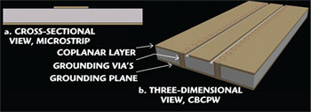
Fig. 1 Cross-sectional view of a microstrip line (a) and three-dimensional view of a CBCPW line (b).
In contrast, microstrip and CPW circuits feature an exposed signal layer, greatly simplifying component assembly on the PCB. Figure 1 shows simple drawings of microstrip and CBCPW transmission lines. The microstrip circuit has a signal conductor on the top of the dielectric substrate and a ground plane on the bottom. In a CBCPW circuit, a coplanar layer with ground-signal-ground (GSG) configuration replaces the signal layer of microstrip. The CBCPW circuit’s top ground planes are tied to the bottom ground plane by means of vias. CBCPW is sometimes known as grounded coplanar waveguide.
In terms of wave propagation, microstrip transmission-line circuits generally operate in a quasi transverse-electromagnetic (TEM) mode. Hybrid transverse-electric (TE) and hybrid transverse-magnetic modes are also possible with microstrip, but these modes are sometimes the result of undesired spurious wave propagation. In general, CBCPW circuits offer propagation behavior similar to that of microstrip circuits.
For both microstrip and CBCPW circuits, spurious parasitic wave propagation can be a problem. As a general rule, the circuit geometry (that is its cross-sectional features) for either transmission-line approach should be less than 45° long at the highest operating frequency of interest. For microstrip, the circuit parameters of concern include the thickness of the substrate (that is the distance between the signal and ground planes) and the width of the signal conductor (transmission line width). For CBCPW, attention must be paid to those two parameters, as well as to the distance between the GSG spacing on the coplanar layer.
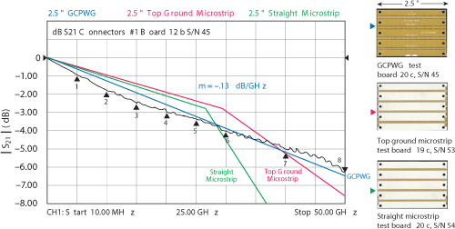
Fig. 2 Comparison of test data for 2½ " GCPWG, 2½ " top ground microstrip and 2½ " straight microstrip test boards.
For proper grounding, CBCPW circuits employ vias to connect the top-layer coplanar ground planes and the bottom-layer ground plane. The placement of these vias can be critical for achieving the desired impedance and loss characteristics, as well as for suppressing parasitic wave modes. When grounding vias are effectively positioned in a CBCPW circuit, a much thicker dielectric substrate can be used at higher frequencies than would be possible for a microstrip circuit at the same frequencies. A review of the practical tradeoffs of via placement for CBCPW circuits is available in the literature.1 Figure 2 offers an overview of signal loss (S21) performance for microstrip, coplanar-launched microstrip, and CBCPW circuits fabricated on 30-mil-thick RO4350B™ circuit-board material from Rogers Corp.
GCPWG refers to a grounded coplanar waveguide and is actually the same configuration as CBCPW. The top ground microstrip configuration is essentially a coplanar-launched microstrip circuit – a microstrip circuit with a CBCPW configuration in the connector signal launch area. The curve-fit data for microstrip and coplanar-launched microstrip are taken from the literature.1 The traces reveal some interesting traits to consider for the different transmission lines. For example, CBCPW typically suffers higher loss than microstrip or coplanar-launched microstrip. The GSG configuration of the CBCPW coplanar layer exhibits higher conductor loss than microstrip-based circuits. Still, the loss for CBCPW follows a constant slope, while the loss curves for microstrip and coplanar-launched microstrip undergo slope transitions at approximately 27 and 30 GHz, respectively. These loss transitions are associated with radiation losses. With proper spacing and via spacing,
CBCPW can be fabricated with minimal radiation loss.
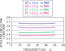
Fig. 3 Effective dielectric constant of a 4 mil LCP laminate with a 50 ohm microstrip line with different surface roughness.
In wideband applications, dispersion can be important. Microstrip transmission lines are dispersive by nature: the phase velocity for EM waves is different in the air above the signal conductor than through the dielectric material of the substrate. CBCPW circuits can achieve much less dispersion when there is tight coupling at the GSG interfaces on the coplanar layer, since more of the E-field occurs in air to reduce the effective inhomogeneity of wave travel through different media.
Using proper design techniques, CBCPW circuits can achieve a much wider range of impedances than microstrip circuits. In addition, applications where crosstalk may be a concern, circuit performance can benefit from the coplanar ground plane separation of CBCPW’s neighboring signal conductors. Due to their significantly reduced radiation losses, dispersion and parasitic wave mode propagation, CBCPW circuits are often used at much higher frequencies than microstrip circuits. At millimeter-wave frequencies, for example, it is often that a simple wire-bonded air bridge will be used to connect the ground planes on both sides of the CBCPW signal conductor. The air bridge approach serves as a “trap” for specific frequencies of concern when spurious wave mode propagation is an issue.2
Copper Surface Roughness
The copper surface roughness of PCB substrates has been known to affect conductor losses as well as the propagation constant of the transmission line.3 The effect on a transmission-line’s propagation constant causes a circuit to have a different “apparent dielectric constant” than expected. Of course, the material parameter is unchanged by the roughness of the material’s metal layer. Rather, the amount of metal surface roughness causes the observed effects by influencing electric field and current flow. As Figure 3 shows,3 the effective dielectric constant can vary widely for the same dielectric substrate when the copper surface roughness is different. The effective dielectric constant increases as the surface roughness of the copper increases, as indicated by copper surfaces with higher root-mean-square (RMS) roughness values.
In addition to observed dielectric constant effects, the surface roughness of a microstrip is known to impact insertion loss performance.3-7 The topology of the circuit may be more or less prone to such copper surface roughness effects, simply due to current and E-field distribution within the circuit. For example, the copper surface roughness has less effect on a tightly coupled CBCPW transmission line than on a microstrip. In a CBCPW circuit, the current and E-field are tightly maintained within the GSG on the coplanar layer. For a microstrip circuit, the field and current move more toward the bottom of the metal, where the roughness lies.
Measuring Differences
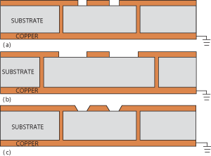
Fig. 4 Cross-sectional views of ideal tightly coupled CBCPW (a), ideal loosely coupled CBCPW (b) and tightly coupled CBCPW with trapezoidal effects (c).
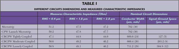
All of the circuits evaluated in this article were fabricated on a 254 µm (10-mil) thick RT/duroid® 5880 laminate from Rogers Corp. The same dielectric material was used in all cases, although with different copper types: rolled copper with surface roughness of 0.4 µm RMS, electrodeposited (ED) copper with surface roughness of 1.8 µm RMS, and high-profile ED copper with surface roughness of 2.8 µm RMS. Table 1 provides details on the dimensions of the different circuits, along with their measured characteristic impedances. The nominal circuit dimensions noted in the table are per the circuit design; however, typical PCB fabrication tolerances apply. On the actual circuits, the signal-to-ground spacing for the coplanar layer of the CBCPW and the copper thickness had appreciable circuit-to-circuit variation.
There is also a real-life issue affecting most PCB circuits and especially CBCPW, which can cause more variation in circuit performance due to standard fabrication effects. This is the conductor trapezoidal effect, or “edge profile,” where the PCB conductors are ideally rectangular in a cross-sectional view but the actual circuits are trapezoidal in shape. This can cause the current density in the coplanar GSG area to vary; an ideal rectangular conductor structure will have more current density up the sidewalls of the adjacent conductors in this region, whereas the trapezoidal structure will have more current density at the base (copper-substrate interface). When there is more current density at the base due to the trapezoidal effect, the copper surface roughness will have more influence on losses and the propagation constant. The trapezoidal concerns for CBCPW PCBs are shown in Figure 4.
Figure 5 compares the effective dielectric constants for two different coplanar circuit types and how they are affected by two extreme cases of copper surface roughness. The phase response measurements that were made for one data set of circuits employed a differential phase length method.8 Circuits were made in very close proximity on the same processing panel and the only difference for the two circuits being measured was the physical length of the transmission lines.
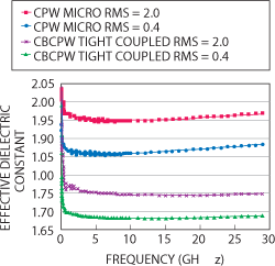
Fig. 5 Effective dielectric constant for two circuit types and two levels of copper surface roughness.
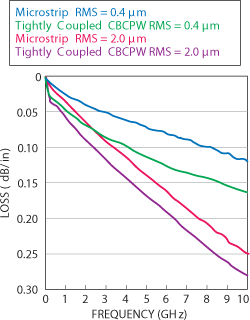
Fig. 6 Comparison of loss between microstrip and tightly coupled CBCPW circuits with different copper surface roughness.
The figure shows that the difference at 10 GHz for the microstrip (cpw micro), for smooth vs. rough copper, RMS = 0.4 vs. RMS = 2.8, respectively, is approximately 0.09 in terms of the effective dielectric constant. The same consideration for the tightly coupled CBCPW is approximately 0.06. Even though trapezoidal effects will cause more variation on the results of CBCPW than for microstrip, the plot shows that the effect of copper surface roughness on propagation constant is much less for CBCPW than for microstrip. The figure also shows a difference in dispersion, where the effective dielectric constant will vary more with frequency for microstrip than for CBCPW. Trapezoidal effects are not considered in the data shown; however, CBCPW circuits could have slightly more dispersion than normal if trapezoidal effects are greater.
Figure 6 shows the insertion loss associated with the two different circuit types and with different copper surface roughnesses. At 10 GHz, the difference in loss for microstrip on rough copper versus smooth copper is approximately 0.250 dB/in. to 0.121 dB/in. For CBCPW, the difference is about 0.280 dB/in. to 0.167 dB/in. The insertion loss performance of CBCPW is less affected by copper surface roughness than the insertion loss performance of microstrip. Trapezoidal effects will have more influence on insertion loss performance for CBCPW than for microstrip.
Simulations and Measurements
To better understand the performance of the circuits studied in this article, models were constructed and analyzed with the help of Sonnet Suite Professional V13.54, a three-dimensional (3D) planar EM simulation software from Sonnet Software. Based on microsectional data from the circuits tested, the simulation geometries, such as substrate thickness and metal surface profile, were entered into the software. An optical coordinate measuring machine (CMM) was used to determine the circuit length accurately. Figure 7 shows an image of one of the CBCPW circuits as it appears in the Sonnet software, while Figure 8 shows a microphotograph of the corresponding cross-section of the circuit.
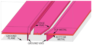
Fig. 7 Isometric view of a CBCPW cross-section in Sonnet.
Fig. 8 Microphotograph of a cross-section of a CBCPW circuit.
While Sonnet contains a native support for modeling thick metal, Figure 7 shows a thick metal approximation drawn manually using the software. Two infinitely thin metals were used in this model, separated by the physical thickness of the metal. The top-layer metal has a width equivalent to the top of the physical metal, and the bottom-layer metal has a width equivalent to the bottom. The layers are then connected with edge vias. This serves to effectively model the thickness of the metal as well as the CBCPW trapezoidal effects — the bottom metal can be seen protruding slightly past the edge via, providing the “sharpness” of the physical profile.
A key to achieving success in the simulation of these types of microstrip and CBCPW circuits is a recently introduced surface-roughness model to V13 of the Sonnet software. The model, which was developed by Sonnet Software’s software engineers in collaboration with Rogers’ material developers, represents a significant advance in metal profile modeling, accounting for the effects on surface inductance of current following partial “loops” in a metal conductor’s profile.9 While it is possible to use the new surface roughness model on the top and bottom of a PCB, it is only applied to the bottom surface of the bottom metal. Roughness is intentionally added only to this physical surface, to aid adhesion to the PCB dielectric material.
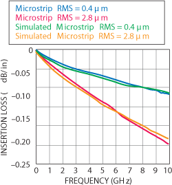
Fig. 9 Simulated and measured microstrip insertion loss.
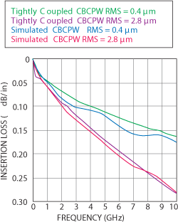
Fig. 10 Simulated and measured CBCPW insertion loss.
Figure 9 offers a comparison between a simulated model and the measured data for microstrip transmission lines. The simulation shows insertion loss for 1". of microstrip transmission line without the connector launch, in order to be a valid comparison with a differential length measurement. Despite working in a scale of only hundredths of decibels, good agreement was achieved between the simulated and measured results for both smooth (0.4 µm RMS) and rough (2.8 µm RMS) metal surfaces. This close agreement provides reassurance of the test setup, the measurement procedure and the validity of the new Sonnet/Rogers surface roughness model.
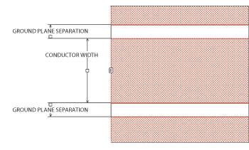
Fig. 11 CBCPW geometry can be broken into three key parameters.
Figure 10 shows similar agreement between simulations and measurements for CBCPW structures. While the agreement for the CBCPW circuits is not as close as that for the microstrip geometries, it is well within the limits of experimental error, confirming the accuracy of the model and the measurements made in this article.
Having established the validity of the surface roughness simulations, it might be beneficial to see how they can be further used in high-frequency circuit design. For example, a common issue with circuit topologies like CBCPW is finding the desired impedance. While many textbook formulas are available for this purpose for conventional microstrip circuits, it is less true for CBCPW circuits. Fortunately, EM simulators are suitable for finding CBCPW geometries for the desired impedance for nearly any reasonable circuit topology. The impedance of a CBCPW design for any PCB material can be broken down to three main parameters: conductor width, material thickness and ground plane separation. As Figure 11 shows, the effects of each of these parameters on CBCPW transmission-line impedance can then be readily analyzed within the EM simulator environment.
Once parameterization is complete, a simulation can be run, which automatically “sweeps” all combinations of the three parameters within a desired range. It is then convenient to plot all impedances on the same graph, allowing a designer to choose the best geometry and impedance from the results. Figure 12 shows an example of such an impedance plot.
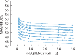
Fig. 12 Example of a "parameter sweep" simulation.
Conclusion
The performance levels of microstrip, CBCPW launched microstrip and CBCPW transmission lines were evaluated under controlled conditions. Both measurements and computer simulations were performed using a commercial, low-loss microwave substrate material with different copper types, including different values of copper conductor surface roughness. The effects of copper surface roughness were evaluated and compared, showing that greater roughness typically means greater loss. Different circuit topologies were compared through both measurements and simulations and, by properly applying computer simulation software, it is possible to reduce the difficulties often encountered with lesser-known circuit topologies.
References
- B.Rosas, “Optimizing Test Boards for 50 GHz End Launch Connectors: Grounded Coplanar Launches and Through Lines on 30-mil Rogers RO4350B with Comparison to Microstrip,” Southwest Microwave Inc., Tempe, AZ, 2007, www.southwestmicrowave.com.
- R.N. Simons, “Coplanar Waveguide Circuits, Components and Systems,” John Wiley & Sons, New York, NY, 2001.
- J.W. Reynolds, P.A. LaFrance, J.C. Rautio and A.F. Horn III, “Effect of Conductor Profile on the Insertion loss, Propagation Constant and Dispersion in Thin High Frequency Transmission Lines,” DesignCon, 2010.
- S.P. Morgan, “Effect of Surface Roughness on Eddy Current Losses at Microwave Frequencies,” Journal of Applied Physics, Vol. 20, No. 4, 1949, pp. 352-362.
- S. Groisse, I. Bardi, O. Biro, K. Preis and K.R. Richter, “Parameters of Lossy Cavity Resonators Calculated by Finite Element Method,” IEEE Transactions on Magnetics, Vol. 32, Part 1, No. 3, May 1996, pp. 1509-1512.
- G. Brist, S. Hall, S. Clouser and T. Liang, “Non-classical Conductor Losses Due to Copper Foil Roughness and Treatment,” 2005 IPC Electronic Circuits World Convention Digest, Vol. 2, S19, pp. 898-908.
- T. Liang, S. Hall, H. Heck and G. Brist, “A Practical Method for Modeling PCB Transmission Lines with Conductor Roughness and Wideband Dielectric Properties,” 2006 IEEE MTT-S International Microwave Symposium Digest, pp. 1780-1783.
- N.K. Das, S.M. Voda and D.M. Pozar, “Two Methods for the Measurement of Substrate Dielectric Constant,” IEEE Transactions on Microwave Theory and Techniques, Vol. MTT-35, No. 7, July 1987, pp. 636-642.
- A.F. Horn, J.W. Reynolds and J.C. Rautio, “Conductor Profile Effects on the Propagation Constant of Microstrip Transmission Lines,” 2010 IEEE MTT-S International Microwave Symposium Digest, pp. 868-871.