
Microwave Journal invited the following contributors to share their tips, tricks and techniques in this month’s cover feature. Call them Gigahertz Gurus or Microwave Merlins, each contributor was asked to offer up some useful advice covering areas such as testing, tweaking and troubleshooting in approximately 500 words or less.
How Low Can You Go
Optimizing Phase Noise
Communication systems rely on a low-phase-noise VCO for reliable voice communications and to ensure transmitted data integrity. As data requirements increase beyond 2 Gb/s, the phase noise of the VCO becomes critical for achieving acceptable bit-error-rate (BER) performance. For low phase noise signal source (VCO) applications, simple tips can cut the design time and be useful for oscillator design engineers.
The frequency tuning feature is realized in an LC resonator VCO by varying the capacitance of the tuning diodes (Varactors). Select low loss resistance varactors and implement back-to-back in the tuning circuit for the minimization of tuning network noise. Care must be taken to avoid breakdown, saturation, or overheating effects in the varactor at the cost of reduced loaded-Q.
Maximize the resonator loaded Q-factor (high group delay); in the series LC-resonant circuits preferably use a large inductor, and in parallel LC-resonant circuits a large capacitor. Care must be taken to suppress the undesired modes in a high Q-factor resonator (especially quartz crystal, ceramic and acoustic resonators) by optimizing the drive-level across the resonator for a given dominant mode.
Use an active device (Bipolar/FET) with low 1/f noise and noise figure at operating frequencies. The trade-off is to use a high frequency transistor that has a small junction capacitance and operate it at moderately high bias voltage to reduce phase modulation due to junction capacitance noise modulation. Care must be taken to prevent modulation of the input and output dynamic capacitances of the transistor, otherwise it leads to amplitude-to-phase conversion and therefore introduces noise.
Since all noise sources, except thermal noise, are generally proportional to the average current flow through the active device, it is logical that reducing the current flow through the device will lead to lower noise levels. The 1/f noise depends on the current density in the transistor, therefore transistors with high Icmax used at low currents will exhibit low flicker noise contribution. In BJTs, as VCE increases, the flicker corner increases as the white noise increases, but the magnitude of the 1/f noise is constant. As base current increases, the flicker corner frequency increases with the magnitude of the 1/f noise and the increased shot noise current. The effect of flicker noise can be reduced through RF feedback. An un-bypassed emitter resistor of a few ohms in a BJT circuit can improve the flicker noise significantly.
Passive components in the oscillator circuit also exhibit short-term instability. Passive components (resistors, capacitors, inductors, reverse-biased, varactor diodes) exhibit varying levels of flicker-of-impedance instability whose effects can be comparable to or higher than to that of the sustaining stage amplifier 1/f AM and PM noise in the oscillator circuit.
Maximize the output RF power carefully; otherwise severe phase noise degradation can occur due to active device noise elevation at compression. For low phase noise, tap the output signal through the resonator to the output load, thereby using the resonator transmission response selectivity to filter the carrier noise spectrum.
The VCO ground plane must be the same as that of the printed circuit board, including adequate decoupling capacitors between the DC supply and ground. Noisy power supplies may cause additional noise. Power supply induced noise may be seen at offsets from 20 Hz to 1 MHZ from the carrier. If the VCO is powered from a regulated power supply, the regulator noise will increase depending on the external load current drawn from the regulator. The phase noise performance of the VCO may degrade depending on the type of regulator used, and also upon the load current drawn from the regulator. To improve the phase noise performance of the VCO under external load conditions, it is always a good design philosophy to provide RF bypassing of power and DC control lines to the VCO.

For ultra low phase noise, use noise reduction techniques: DC noise-feedback, mode-coupling, injection-locking, degenerative noise filtering, feed-forward and other noise reduction techniques. Narrowing the current pulse width in the active device will decrease the time that noise is present in the circuit and therefore, decrease the effective noise factor for a given drive-level and minimize the phase noise.
Dr. Ajay Poddar, Chief Scientist
Ajay is Chief Scientist at Synergy Microwave where he is responsible for design and development of state-of-the-art RF modules such as oscillators, synthesizers, antennas, mixers, amplifiers, filters, and MEMS based RF components.
Showing Bias
GaN HEMT PA Gate Currents
GaN HEMT based power amplifiers (PA) can have somewhat different compression characteristics compared to other RF semiconductor based PAs. Depending on the setting of the quiescent drain current they often will have soft compression characteristics. Very often a conventional P1dB metric is not valid for a GaN HEMT PA since the real criteria are peak output power, two-tone nonlinearity and spectral re-growth which may depend more on Psat than P1dB. Of course,
AM-PM characteristics will matter in the nonlinear performance of the PA but, again, GaN HEMT transistors tend to have rather different AM-PM characteristics versus output power than, say, Si LDMOS FETs or GaAs MESFETs. As Psat is approached, the AM-PM curve versus output power will often “turnover” (i.e., a negative going phase change will become positive going).
In unison with such behavior the gate current of the GaN HEMT transistor as a function of RF input power will also undergo a change so it is worth monitoring the magnitude and “sign” of the gate current. This monitoring will allow the designer (particularly at the prototyping stage) to know when the PA is getting close to its Psat condition. The gate bias supply must be able to source and sink current (i.e., reverse and forward current). Cree has an application note on its website called “GaN HEMT Biasing Circuit with Temperature Compensation”1 that indicates the desirable features of a typical biasing arrangement. In most cases (e.g., Class A/B), the gate current will have a negative value at RF output power levels that are less than Psat. As Psat is approached the negative gate current will reach its maximum value and then reverse and go positive. This is due to the HEMT Schottky diode starting to be overdriven by input RF swings. The data sheets on all Cree GaN HEMT devices provide a maximum forward gate current that the designer needs to be aware of. In the case of one of our 25 W transistors,2 this value is 7 mA. Although no damage will be done to the transistor for short periods of time if this forward gate current limit is somewhat exceeded, it is always considered that the limit be respected and is an excellent indicator that the device has reached its Psat output power. Incidentally, the RF input power level at which the gate current “flips” its direction is almost coincident with the AM-PM phase characteristic reversal. Clearly, there are other nonlinearities taking place in the device such as gate-to-source capacitance and source resistance that also effect the AM-PM characteristics.

Ray Pengelly, Strategic Bus. Dev. Manager
Ray is responsible for wide bandgap technologies for RF and microwave applications among Cree RF and microwave products.
- www.cree.com/~/media/Files/Cree/RF/Application%20Notes/Appnote%2011.pdf
- www.cree.com/~/media/Files/Cree/RF/Data%20Sheets/CGH40025.pdf
Filter This
Calculating Coupling
In memory of my father, Aharon Hershtig (1927-2012), a Holocaust survivor, a strong and sensitive person, who inspired me.
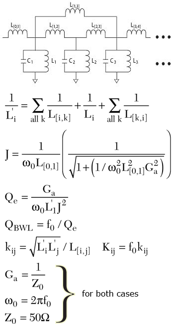
Extracting coupling values (known by technicians as “loading bandwidths”) from filter networks is essential for tuning filters and troubleshooting. In the early 90s, wireless communication called for bandpass filters in basestations to exhibit elliptic responses with sharply skewed rejection skirts, exemplified by the Tx/Rx duplexer. Following the filter design recipe book, the first step was to find the lowpass prototype network and use its g-values to calculate external and internal coupling values. While the desired bandpass was asymmetric and sharply skewed to one side, the transformation from lowpass to bandpass is symmetric. As a last resort, many filter designers started with an all-pole network, introduced and refined cross couplings via optimization with a linear simulation tool, and extracted coupling values from the network very much as they would do on the bench when prototyping filters. A select few companies, such as those that had supplied filters to the satellite communication market in the 70s and 80s and those with university professors on staff, had access to skills and computer programs for directly synthesizing elliptical bandpass filters and easily extracting coupling values using matrix manipulations. For those outside that group, it was essential to develop generalized formulas for calculating coupling values for arbitrary elliptic response networks.
Since coupling values could be easily computed from g-values for all-pole networks, it seemed reasonable that practical formulas might exist in analogous form for asymmetrical networks. Further, most of the sophisticated direct synthesis programs could deal with just one doubly-terminated channel and couldn’t take into account multiple filters connected to a junction. When real estate doesn’t permit the “phasing” of filters, as with most basestation filters, external couplings and some internal couplings have to be adjusted. Deviation from the doubly-terminated condition depends on rejection at the crossover frequencies. If two filters are duplexed together and brought as close as 3 dB at crossover, coupling values will change dramatically from the doubly-terminated to singly-terminated case.
Generalized Coupling Formula – Inductor
External and internal coupling values for inductive coupled parallel LC resonators:
Generalized Coupling Formula – Capacitor
External and internal coupling values for capacitive coupled parallel LC resonators:
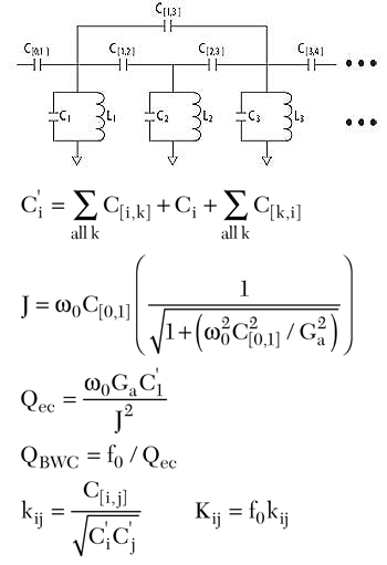

Once filters are simulated using lumped elements, coupling values can be calculated for any scenario for implementation with any technology, including TEM, TE, etc. In the mid 90s, Kevin Asplen and I wrote a program at K&L Microwave to extract coupling values from directly synthesized networks produced by S/Filsyn and other design tools and duplexed and optimized with various linear simulators. The “black magic” was gone. Tuning and troubleshooting filters became much easier.
Rafi Hershtig, VP of Advanced Engineering and R&D
Rafi continues to evolve the state of the art in filter design at K&L Microwave through innovations that lead to improving performance, shrinking the footprint and integrating capabilities.
Gimme More
Amplifier Bandwidth
Published literature and conference sessions are booming with techniques for maximizing efficiency, improving linearity, reducing size, etc. of amplifiers, but often these techniques come at the sacrifice of bandwidth. An ideal solution could realize these performance enhancements without reducing the frequency response. Designing for the widest bandwidth possible requires subtlety.
Start with good active models.
Although foundry transistor models have become much better in recent years, they are made to appeal to the widest audience possible. This “one model fits all” approach works for narrowband applications (i.e., add a few tunable components for the bench test and you’re golden). For wideband applications, you need transistor models that provide accuracy over the entire frequency range of interest. Creating a scalable, wideband behavior model that represents thermal effects (resistive and capacitive), process variation (i.e., supports Monte Carlo), and bias dependency is non-trivial. Before starting a wideband design, always compare the model against measured data. If the model is not accurate over the entire range of interest (with some margin), extract a custom model.
Start with good passive models.
Similarly, passive models have become much better in recent years. Component-level parasitic effects are the most limiting factor in achieving wide bandwidth. Substrate permittivity, mounting orientation, proximity to ground plane, and self-resonance are some of the parasitic effects often overlooked. If models with this level of detail are not available, mount the component in a representative fixture (i.e., use the same substrate as the final product), measure S-parameters, de-embed the fixture, and use the measured results in simulation. For a more versatile solution, have a custom model made (I use the Modelithics scalable model).
Create your own N-section transformer.
A common way of achieving wide bandwidth matching networks is with N-section transformers, where N is usually 2, 3 or 4. The three most popular algorithms are exponential, equal ripple, and maximally flat (listed from widest bandwidth with most ripple to narrowest bandwidth with least ripple). Using these three configurations as a starting point, the Smith Chart Utility in Agilent ADS is a powerful tool for tweaking the section impedances to find the right balance of bandwidth and ripple that works for the application (seek the Microwaves101.com free Excel calculator to get started). To minimize size, meander the RF traces and/or replace transmission lines with lumped components.
Know the system need.
Fact: Amplifiers have less gain, power, and efficiency at higher frequency than lower frequency. To achieve equal performance across a wide frequency band, low-end performance is worsened to match the high end. When designing for extremely wide bandwidths (i.e., multiple octaves or decades), this can amount to a significant degradation at the low end (i.e., -6 dB gain per octave adds up quickly). Is a flat response really necessary? Somewhere in the front-end is an antenna with positive gain per octave. Negative amplifier gain slope over frequency could be a benefit!

Know the limiting factor.
In every system, there is a bandwidth-limiting element. Always know what it is. Often, packaging is the culprit. Watch for practical limitations from feedback circuits and reactive matches. Passive components, like couplers and splitters, usually have well-defined band edges (especially when wideband). In general, any technique using a phase shifter is going to be bandwidth limited. When exploring the widest bandwidth possible, knowing the limiting factor will allow the designer to focus on the greatest area of constraint.
Dr. Nickolas Kingsley, Director of Engineering
Nick manages the engineering team at Auriga Microwave. His research interests include the design, miniaturization, fabrication, packaging and testing of RF MEMS multilayer front ends.
Distorted Tones
Measurement Fidelity
Third order distortion measurements such as intermodulation distortion (IMD) and third order intercept (IP3) at high power levels (think IP3 at +40 dBm and higher) are often some of the most difficult RF measurements to make. Often, these measurements require careful attention to minimizing the IMD products of both the source signal and the RF signal analyzer. Here are a few important tips for creating the best possible source signal and for squeezing the last few dB out of your signal analyzer.
Let’s start with the source, typically consisting of two RF signal generators and a combiner network. Here, one of our primary concerns to isolate the sources to prevent RF energy from leaking between them – a problem that could ultimately produce IMD products in the test signal. While choosing a combiner with excellent port-to-port isolation (like a Wilkinson power combiner) is a good start, getting the best source isolation requires a little more effort.
There are several methods to improve source isolation – each with varying degrees of effectiveness and difficulty. Couplers and isolators are the simplest technique to get an additional 30 to 40 dB of isolation – but are generally only effective within one frequency octave. When setting up a broadband test bench, an amplifier (with high reverse isolation) or attenuator (or both) placed between each signal source and the power combiner can be a highly effective technique to isolate each source to produce the best two-tone signal.
Once you’ve set up a clean two-tone source, the next step is to analyze the IMD products of both the stimulus signal and the RF signal analyzer. Here, squeezing out the last few dB of dynamic range requires a basic understanding of the receiver’s architecture. Generally, you’ll first want to control the analyzer’s front-end attenuation either manually or by setting the reference level. An easy way to determine if your RF signal analyzer is contributing its own distortion is to slowly increase the front-end attenuation while observing IMD products. If the IMD products decrease in power as attenuation increases, you can quickly deduce that your instrument is contributing to the measurement error. However, if IMD products remain constant with an increase in attenuation, you can be certain that these intermodulation products are inherent to the signal source. Eventually, too much attenuation will begin to raise the noise floor of the instrument and you’ll need to either reduce resolution bandwidth or apply averaging to continue to observe IMD products.
If you determine that IMD products are the result of the RF signal analyzer’s linearity, a second technique to further improve the analyzer’s linearity is to condition the signal at the intermediate frequency (IF). Often, the linearity of the IF digitizer of the instrument is a major contributor to distortion products. Thus, one can improve the linearity of the instrument by setting a narrow IF bandwidth and ensuring that the frequency spacing of the two-tone signal exceeds the bandwidth of the IF filter.

Once you’ve verified that both the source and receiver have IMD levels that are low enough to make your measurement, it’s time to connect your DUT. Of course, remember that you’ll want to increase the reference level or attenuation of the RF signal analyzer by the expected gain of the DUT to ensure that you’re operating the receiver at the same power level you’ve optimized it for already. Finally, you’re ready to measure the power of both the 1st and 3rd order distortion products to determine IP3 or IMD performance of your DUT.
David A. Hall, Senior Product Manager
At NI, David applies his expertise in digital signal processing and communications systems to develop product demos, provide user feedback, and write application notes.
Stable as a Rock
Spurious Oscillations
Amplifier instability can show as spurious (unwanted) signals in the frequency domain, sometimes only visible when there is a (wanted) output signal, at other times they can appear as noise ‘humps’ or unexpected decreases in output power or gain – appearing like a ‘bite’ out of the frequency response. Although in a system context they may be tolerable (low enough or in a non-interfering part of the spectrum) they are indicative of a design that could be better controlled. We are not considering switching frequency sidebands, which may appear on the output signal through the bias circuits, but frequencies produced within the devices themselves. If it looks like ohms law isn’t working – search for oscillations. The normal approach to stable amplifier design is to consider the ‘k’ factor. However, this will only address a group of oscillations referred to as even mode, and to comprehensively account for these, one should consider the behaviour of the device during switch on and at all the input drive levels. This is because the calculations for k depend on device transconductance and parasitic elements, many of which are input power level and bias dependant. Odd mode oscillations occur within the combining loops of parallel transistors that make up power devices and MMICs. They may not even directly appear at the device output.
Essentially to prevent oscillations, gain must be reduced at the frequency(s) concerned, which tends to oppose one of the key design aims, hence it must be applied in a frequency selective manner. On the input, some series resistance can be tolerated and may make matching easier, but this is rarely acceptable at the output. Series negative feedback is commonly applied in low noise amplifiers where it can have the added benefit of bringing into line the input match and optimum noise figure impedance, but is impractical for power designs. Shunt feedback can be employed to flatten gain and used with bias line de-coupling to produce highly stable amplifiers. Care must be taken with the bias line connections, particularly coupling between stages, where positive feedback is possible; hence, it is important to analyze such structures over the full bandwidth from DC to the maximum operating frequency of the device. To this end the bias decoupling should include resistive loss and a sufficient range of capacitor values. Although the main RF decoupling capacitor should be low loss, higher loss dielectrics can usefully be employed for the lower frequencies. Do not share via holes to ground on decoupling capacitors; good solid grounding, although going against some standard design rules (thermal breaks), reduces inductance.
Signals don’t always flow the way you want them, and physical constraints mean that the cavity is often larger than we would like. In this case, we need to reduce the risk of modes being started (launched) and ensure they are attenuated as quickly and as much as possible. High impedance lines should be realized in coplanar waveguide, if possible, containing the radiated fields. Pillars grounded at both ends can be erected within the cavity to break up box modes. The judicious use of Radar Absorbent Material (RAM) is not ‘applying bandages’ as some would see it, but a valid technique.

Testing needs to be carried out across the range of input power and load impedances, and also the full temperature range, especially cold where gain is highest and spurs are likely to be encountered. Low temperature oscillations may be removed by powering up the amplifier in advance of use, raising the temperature sufficiently.
Dominic FitzPatrick, Principal Consultant
Dominic is a specialist in RF and microwave solid state amplifiers. As Technical Director of two British microwave amplifier companies, he was responsible for technological innovation and new product development, serving customers worldwide www.powerful-microwave.co.uk
Making Cents
E-Band Modules
At frequencies up to around 40 GHz, the vast majority of RF components are supplied in Surface Mount Technology (SMT) packages. Components operating in the un-licensed 60 GHz band and at E-Band will ultimately also be available in SMT packages, but this requires advances in both chip-scale packaging technology and PCB technology. Current commercially available components addressing these bands are normally supplied as bare die and one of the first challenges to the user is routing RF signals to and from the die without suffering serious performance degradation.
A 1 mm length of bondwire has an inductive reactance of around 340 Ω at 60 GHz and 486 Ω at the top of E-Band (71 to 76 GHz and 81 to 86 GHz). At these frequencies, bond interface parasitics can seriously degrade the performance of a die and must be minimized. The first step is to ensure that the surface of the interface substrate is at the same level as the surface of the ICs. There are essentially two practical approaches; both require the use of a substrate material of similar thickness to the die. The first approach is to use a hard substrate (such as quartz or alumina). In this case, the substrate and die can be butted up to minimize bonding distances but multiple substrates may be required resulting in a more complex assembly. The second approach is to use a soft substrate (such as LCP or RT Duroid) with holes cut into the substrate into which the die can sit. This allows a single interface substrate but tolerances on hole dimensions can increase bonding distances.
The inductance of the bond itself can be reduced by using multiple parallel wires or tape bonds instead of wire. Direct die to die bonding offers the ultimate in minimizing bonding distances and parasitics. Bonding of the ground pads as well as the signal pads can improve the performance of the transition. If tape bonding is not available, two parallel wire bonds can provide acceptable performance. When bonding from the die to a microstrip track on the interface substrate, the wider substrate track allows the formation of a “v” bond, which will reduce the mutual inductance.
Many of the datasheets for mm-wave die recommend the use of Single Layer Capacitors (SLC) for de-coupling. These are much more expensive than SMT capacitors and require wire-bond assembly. In fact, this approach is often a hang-over to the days of microwave chip and wire assembly. SLCs do offer high capacitance with low parasitics but a well designed mm-wave IC will have adequate on-chip decoupling for the microwave and mm-wave frequency range. At RF frequencies and below, for which the higher value de-coupling capacitors are actually required, inexpensive SMT capacitors are often perfectly adequate. The effectiveness of this approach should be confirmed with appropriate trials but it can reduce cost and complexity without sacrificing performance.

For E-Band and 60 GHz assemblies aimed at volume production, the largest potential cost saving can obtained by developing custom MMICs. E-Band LNAs fabricated on 0.1 µm gate length PHEMT processes cost over $100 in 1000-off quantities. Parts of the same die area can be produced on commercially available foundry processes for around $5. This excludes the NRE development costs but for a high volume application this is soon amortized with production.
Liam Devlin, Director of RF Integration
Liam has led the design and development of over 70 custom ICs on a range of GaAs and Si processes at frequencies up to 90 GHz for Plextek Ltd., a UK design consultancy.
Tricky Trade-offs
Doherty Power Amplifiers
Doherty power amplifiers (PA) use main and auxiliary (peaking) amplifiers, connected in parallel, to attain relatively high efficiency over a range of output powers. Designing one can be a tricky proposition since there are many different parameters to be adjusted and multiple responses to look at, most of which are specified versus the output power, which unlike the input power is also a response from the simulation. In order to make the trade-offs necessary to meet specifications over a wide range of output powers, the engineer must determine which parameters have a dominant effect on performance.
A number of techniques can be employed to improve Doherty PA performance. Sweeping one parameter at a time allows the engineer to sweep an arbitrary parameter in the design and see how the performance varies. This provides quick insight into whether or not a specific parameter has any effect on performance, this technique is a reasonable first step to take when trying to understand and improve Doherty PA performance. Sweeping two parameters at a time extends the single parameter sweep to provide an effective means of understanding the interaction between two parameters. Results can be viewed on contour (and other) plots.
Design of Experiments (DOE) varies many different parameters simultaneously, while keeping track of the results. It quickly lets the engineer know which parameters most strongly influence performance. Examining one parameter at a time to gain such information would be too tedious and time consuming. On the downside, some time and effort is required to set up this technique’s methodical simulations and DOE is not supported by all CAD tool vendors.
Optimization is a common approach to improving amplifier performance. Somewhat simpler to set up than DOE, it is automated and can run for an indefinite length of time. However, it must combine all goals together to create a single error function. Although it may produce reasonable results, it doesn’t provide insight into what trade-offs are being made to reduce error. Additionally, optimizers can get stuck while systematically searching through the design space. Some engineers find value in using both DOE and optimization.
Monte Carlo (MC) analysis is much like running a multi-dimensional parameter sweep, this novel technique investigates the sensitivity of the amplifier’s performance to as many parameters as the engineer desires. Two types of parameters can be simulated: design variables, which the engineer can control, and random variables (e.g., foundry statistical variables), which the engineer cannot control. Because this technique samples a lot of points at random, a more thorough or complete sampling of the solution space can be achieved. The computing cost is independent of the number of random variables. On the downside, it requires some post processing and additional effort to obtain correlations. Advanced Design System (ADS) from Agilent, for example, has example data display files set up to show these results. Most tools support the technique itself, but may not offer added post processing or correlation capabilities. MC will not necessarily provide better results than DOE.

While each of these techniques has some value, the general rule of thumb is to first run a single and/or double parameter sweep. If doing so provides feedback that a design can satisfy all of its specifications, then the job is done. If not, the next step is to employ DOE or MC, or perhaps even run both in that order. At the end of the day, if the Doherty PA is unable to meet all of its specifications, then the data obtained from either of these techniques can be used as the basis of further discussion with the system designer regarding trade-offs in the specifications.
Andy Howard, Senior Applications Engineer
Andy currently focuses on power amplifier simulation techniques for Agilent Technologies, working with many different applications of Agilent’s ADS, RFDE and GoldenGate simulators.
Yer Done Son
When to Stop Engineering
The key to achieving expedient first pass design success with filters is to use both software and test and measurement tools as efficiently as possible. In most cases, “efficiency” is nothing more than cutting out unnecessary design steps, automating tedious steps, and ultimately knowing when to “stop engineering.” Below are tips to avoid getting caught in infinite design iterations.
Overdesign for return loss and ignore insertion loss.
Return loss is always worse in real life due to discontinuities. By leaving at least 5 dB of margin, the real life design will be acceptable. Conversely, ignore insertion loss because accurately modeling such physics is computationally intensive. As for insertion loss, “it is what it is.” Don’t fight it in the first pass. If insertion loss matters, use low surface roughness options like rolled copper, it makes a huge difference.
Learn your fabrication technology’s tendencies.
Learning tendencies of the fab house requires experience, so pay attention to every design iteration and record the trends. We find that when we send our filter designs out, the center frequency tends to be about 100 to 200 MHz off and the bandwidth is reduced a little (say from 7 to 5%). Compensating for the fab drift allows us to do custom filter work in a matter of days, instead of months.
Above a few, ghz lumped elements don’t act like lumped elements.
Inductors are the worst, followed by capacitors and resistors. We limit the use of chip inductors to designs below 6 GHz but use capacitors and resistors beyond 40 GHz. For lumped elements, the smaller the better. If you insist on simulating Rs, Ls and Cs above a few GHz, consider including the parasitic reactance, and pray the models are correct.
When debugging, blame yourself first, and blame the vendors last.
When you build your prototype and it doesn’t work, first assume you made a mistake. In RF, the two most common mistakes are connector transitions and grounding issues. Another potential error source is forgetting to simulate something. Issues like connector transitions and metal lids can wreak havoc on your delicate circuitry, and circuit solvers typically ignore these effects. Debugging should be systematic, and assuming the vendor made a mistake is a last resort option rife with peril. Vendor mistakes happen occasionally, design mistakes happen daily.

When to stop engineering.
The biggest waste of time is fighting for a few tenths of a dB in software. Time is money, and sometimes it is cheaper to release the design, build a prototype, take measurements, and then go back to the software only after you get your sanity check. Don’t fall in love with your CAD software, sometimes it lies! Real life testing will keep your software honest.
Chris Marki, Director of Research
Chris is responsible for the design and commercialization of many of Marki’s fastest growing product lines.