
Due to the fast growing demand for broadband wireless communications, the operating frequency band is moving toward the 5 GHz U-NII band. The advantage of combining baseband and the RF front-end on one single chip for cost savings is strongly desired for highly integrated systems-on-chip (SoC) applications. Due to the improvements of the standard CMOS process, the unity gain frequency fT of CMOS devices becomes comparable to that of GaAs. Recently, many RF circuits realized in the CMOS process have been reported and the 0.18 µm process is a good candidate for highly integrated SoC applications.1 The requirements of low power and low cost push the trend toward the goal of a radio-on-a-chip (RoC).
For an 802.11a WLAN application (5.725 to 5.825 GHz), a proposed heterodyne receiver architecture is shown in Figure 1. The RF (5.725 to 5.825 GHz) is downconverted to an IF of 280 MHz by a first LO (5.445 to 5.545 GHz) and is then further translated to zero by a 280 MHz LO to produce I and Q baseband components. In order to increase the linear gain and save power consumption, a current-reuse technology is adopted2 instead of a conventional cascode LNA. Two topologies of current-reused LNA have been reported. One is made of inductively degenerated NMOS and PMOS pairs in shunt configuration to achieve current reuse.2,3 Its linearity is of concern because of the different mobility of NMOS and PMOS devices. The other topology is made of a two-stage, common source amplifier to share the operating current and reduce current consumption.4,5 In this article, a current-reuse topology consisting of a two-stage, common source amplifier is adopted for the LNA design to share the operating current.4 The 5.7 GHz LNA is fabricated in a TSMC 0.18 µm standard CMOS process.
 | ||
| Fig. 1 Proposed 802.11a WLAN receiver architecture. | ||
LNA Topology and Circuit Design
Figure 2 illustrates the LNA with a current-reuse topology. For the low power consumption requirement, the two-stage amplifier is folded into a single stage. It means that it is cascode for DC and cascade for RF signals. The two cascading common source amplifiers share the same supply current to reduce power consumption. Hence, with the same gain performance, this circuit only consumes about half the power of the two-stage amplifier. C1 is a coupling capacitor, L1 is an RF choke and C2 is a capacitor providing AC ground. In this topology, the Miller effect is more serious than in a cascode amplifier, since the first common source amplifier has a large voltage gain. This effect can be reduced by inserting an inductor before the gate of the second stage. The input impedance of the LNA is matched to 50Ω since the bandpass filter (BPF) required in most conventional receiver architectures is in a 50Ω system. The source degeneration method6 for input matching is employed and is shown in Figure 3. Lg and LS can provide a 50Ω input matching.
 | ||
| Fig. 2 CMOS LNA with a current-reuse topology. | ||
 | ||
| Fig. 3 Source degeneration topology for input matching. | ||
The circuit schematic of a 5.7 GHz CMOS LNA is shown in Figure 4. In the CMOS LNA, design considerations include linearity, stability, noise figure, input and output matches, and DC bias. For low power consumption requirements, the DC current is set as low as possible. When the DC operating point is determined, the most important procedure is to choose the optimal NMOS transistor channel width that has the lowest noise figure,6 and the gate-to-source capacitance (Cg) can then be derived. While the input impedance is 50Ω, the inductance of Lg and Ls can be derived as

where
gm1 = transconductance of M1
Cg = gate-to-source capacitance of M1
Lg = input inductor of the gate
Ls = source-degeneration inductor
Since the values of Lg and Ls are not very large, they can be realized by a well-controlled bond-wire with high Q value. An Ls with a high Q value is beneficial to the low noise performance. C1 is an off-chip DC blocking capacitor. The Q value of an off-chip capacitor is higher than for an on-chip metal-insulator-metal (MIM) capacitor, and the noise figure can be reduced. C2 and C3 are coupling capacitors implemented by MIM capacitors. L1 is an on-chip spiral inductor for an RF choke. Lchoke is realized by a bond-wire for choking the RF signal. L2 is an on-chip spiral inductor for inter-stage matching. C4, L3 and L4 form an output matching network, while L3 and L4 are realized by well-controlled bond-wires. Figure 5 shows the LNA layout.
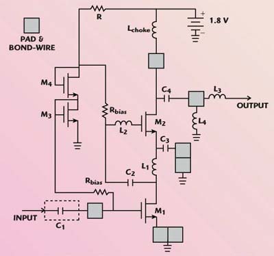 | ||
| Fig. 4 Schematic of a 5 GHz LNA with current reuse. | ||
 | ||
| Fig. 5 5.7 GHz CMOS LNA layout. | ||
Measured Results
 | |||
| Fig. 6 5.7 GHz CMOS LNA on an FR-4 PCB test fixture. | |||
Agilent Advance Design System (ADS) is used for circuit simulation. The measurements are performed on an FR-4 PCB test fixture, as shown in Figure 6. The LNA chip is connected to the test board with aluminum bond-wires. The equivalent inductance of the bond-wire is approximately 1 nH/mm. The effects of bond-wires and the FR-4 test board have been taken into account in the circuit simulation. The parasitic capacitance to ground is larger than for a conventional test fixture, since the die is mounted on the ground plane directly. By considering this effect, the input and output parasitic capacitance are modeled as 0.1 and 0.2 pF shunted to ground.
The CMOS LNA measurement results are shown in Figure 7. The input and output return losses are approximately 10.5 and 5.6 dB at 5.8 GHz, respectively. The gain is approximately 11.2 dB and the two-tone test shows that the OIP3 is approximately 9.8 dBm. The noise figure is 4.5 dB and the input P1dB is –10 dBm. Table 1 shows the summary of the simulated and measured performance of a 5.7 GHz 0.18 µm CMOS LNA.
 | ||
| Fig. 7 Measured performance of a 5.7 GHz CMOS LNA with current reuse; (a) input return loss, (b) output return loss, (c) gain and (d) two-tone intermodulation. | ||
 | ||
Conclusion
This article presents the design, implementation and measurement of a 5.7 GHz CMOS LNA for an IEEE 802.11a WLAN receiver application. The LNA with a current-reuse topology to increase linear gain and save power consumption is fabricated in a TSMC 0.18 µm 1P6M CMOS process. The measurements are performed by using an FR-4 PCB test fixture. The fabricated LNA exhibits a linear gain of 11.2 dB, a noise figure of 4.5 dB, input/output return losses of 10.5 and 5.6 dB, an input P1dB of –10 dBm and an OIP3 of 9.8 dBm at 5.8 GHz. The power consumption is 14.4 mW at VDD = 1.8 V.
Acknowledgment
The authors would like to thank the Chip Implementation Center (CIC) of the National Science Council, Taiwan, ROC, for its support of the TSMC CMOS process.
References
-
T.H. Lee, The Design of CMOS Radio-frequency Integrated Circuits, Cambridge University Press, New York, NY 1998.
-
H. Fouad, K. Sharaf, E. El-Diwany and H. El-Hennawy, “An RF CMOS Cascode LNA with Current-reuse and Inductance Source Degeneration,” Radio Science Nineteenth National Conference Proceedings NRSC 2002, pp. 450–457.
-
F. Gatta, E. Sacchi, F. Svelto, P. Vilmercati and Rinaldo Castello, “A 2 dB Noise Figure 900 MHz Differential CMOS LNA,” IEEE Journal of Solid-state Circuits, Vol. 36, No. 10, October 2001.
-
C.Y. Cha and S.G. Lee, “A Low Power, High Gain LNA Topology,” International Microwave and Millimeter-wave Technology Conference, 2000, pp. 420–423.
-
K. Yamamoto, T. Heima, A. Furukawa, M. Ono, Y. Hashizume, H. Komurasaki, H. Sato and N. Kato, “CMOS Low Noise/Driver MMIC Amplifiers for 2.4 GHz and 5.2 GHz Wireless Applications,” Silicon Monolithic Integrated Circuits in RF Systems, 2001, pp. 18–22.
-
D.K. Shaeffer and T.H. Lee, “A 1.5 V 1.5 GHz CMOS Low Noise Amplifier,” IEEE Journal of Solid-State Circuits, Vol. 32, No. 5, May 1997, pp. 745–759.
 Liang-Hui Li received his MSEE degree from National Cheng Kung University, Tainan, Taiwan, in 2002. He worked on 802.11a RF system planning and 5 GHz CMOS RFIC circuit design for his master study. He is currently with the Realtek Semiconductor Corp. as an R&D engineer. His research interests include RF system and RFIC design for wireless communication systems.
 Huey-Ru Chuang received his BSEE and MSEE degrees from National Taiwan University, Taipei, Taiwan, in 1977 and 1980, respectively, and his PhD degree in electrical engineering from Michigan State University, East Lansing, MI, in 1987. From 1987 to 1988, he was a post-doctoral research associate at the Engineering Research Center, Michigan State University. From 1988 to 1990, he was with the Portable Communication Division of Motorola Inc., Ft. Lauderdale, FL. He joined the department of electrical engineering at National Cheng Kung University, Tainan, Taiwan, in 1991, where he is currently a professor. His research interests include antenna and RFIC/microwave circuit design for wireless communications, computational electromagnetics and applications, EMI/EMC, microwave communication and detection systems.