
Due to the fast growing demand for broadband wireless communications, the operating frequency band is moving toward the 5 GHz U-NII band. The advantage of combining baseband and the RF front-end on a single chip for cost savings is strongly desired for highly integrated systems-on-chip (SoC) applications. Due to improvements of the standard CMOS process, the unity gain frequency fT of CMOS devices becomes comparable to that of GaAs. Recently, many RF circuits realized in the CMOS process have been reported and the 0.18 µm process is a good candidate for highly integrated SoC applications.1 The requirements of low power and low cost push the trend toward the goal of a radio-on-chip (RoC).
 | |||
| Fig. 1 IEEE 802.11a frequency allocations; (a) WLAN and HYPERLAN and (b) upper sub-band WLAN. | |||
With a maximum data rate of 54 Mbit/s, the IEEE 802.11a wireless LAN (WLAN) standard specifies a 300 MHz spectrum allocation at 5 GHz that is divided into three sub-bands, as shown in Figure 1. The lower and middle U-NII sub-bands, from 5.15 to 5.35 GHz, accommodate eight channels in a total bandwidth of 200 MHz. The 100 MHz bandwidth of the upper U-NII band, from 5.725 to 5.825 GHz, accommodates four channels. The 100 MHz lower U-NII band is restricted to a maximum power output of 40 mW, and the middle and upper sub-bands are restricted to 200 and 800 mW, respectively. The 802.11a WLAN frequency allocation overlaps with HIPERLAN from 5.15 to 5.3 GHz. For 802.11a WLAN applications (5.725 to 5.825 GHz), the proposed heterodyne receiver architecture is shown in Figure 2. The RF (5.725 to 5.825 GHz) is downconverted to an IF of 280 MHz by a first LO (5.445 to 5.545 GHz) and then is further translated to zero by a 280 MHz LO to produce I and Q baseband components.
 | ||
| Fig. 2 Proposed receiver architecture for an 802.11a WLAN upper sub-band application. | ||
The down-conversion mixer is one of the key components of the RF receiver and determines the quality of the received signal. An active mixer is a compromise between linearity and conversion gain. Usually, the active mixer is a Gilbert-cell mixer or a single-balanced mixer. A Gilbert-cell mixer has a better LO-to-IF isolation than a single-balanced mixer, but requires more power consumption and has a higher noise figure. On the contrary, a single-ended mixer suffers from a poor LO-to-IF isolation and the IF circuits may have to handle a high power LO leakage if the LO is not attenuated sufficiently by an IF filter. Nevertheless, for the RF front-end shown, the LO frequency is much higher than the IF; the LO signal can be easily filtered out. Hence, a single balance topology is used for the CMOS mixer. This article presents the design of a 5 GHz single-balanced mixer fabricated in a TSMC 0.18 µm standard CMOS process.
Mixer Circuit Design
Figure 3 is the schematic of a single-balanced mixer,3 where VRF is the input at the RF port and VLO± are the inputs at the LO ports.
 | |||
| Fig. 3 Single-balanced mixer architecture and operating principle. | |||
The function of M1 is to transfer the received RF signal (VRF(t) = nRFcoswRFt) from voltage to current![]()
The transistors M2 and M3, controlled by the LO (VLO±(t) = ±![]() LOcos
LOcos![]() LOt), act as switches to modulate the current provided by M1 with a square wave the frequency of which is
LOt), act as switches to modulate the current provided by M1 with a square wave the frequency of which is ![]() LO. The ouptut current of the mixer is
LO. The ouptut current of the mixer is
![]()
where
sgn = a square wave of amplitude ±1 and frequency ![]()
Using Fourier series to expand sgn[cos![]() LOt] yields
LOt] yields

By ignoring the high order terms, the output IF signal can be written as

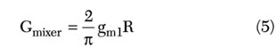
Therefore, the voltage conversion gain of the mixer, Gmixer, is independently set by the transconductance of M1 and the load resistance, and can be written as
The drawback of the single-balanced mixer is the poor LO-to-IF isolation. According to Equation 4, the IF output of the mixer has a (4/![]() )IbiasRcos
)IbiasRcos![]() LOt term, which is the LO leakage. But, in a system where the LO frequency is much higher than the IF, the LO signal can be filtered out with an IF filter. The LO-to-RF isolation is primarily controlled by the balance between M2 and M3 transistors and the LO balance. The LO-to-RF isolation is ideally infinite.
LOt term, which is the LO leakage. But, in a system where the LO frequency is much higher than the IF, the LO signal can be filtered out with an IF filter. The LO-to-RF isolation is primarily controlled by the balance between M2 and M3 transistors and the LO balance. The LO-to-RF isolation is ideally infinite.
The transconductance, noise figure and linearity of the mixer are mostly governed by M1. Considering the power consumption and the above mentioned parameters, the width of the M1 was chosen to be 200 µm. The transistors M2 and M3 are acting as a switching pair. The switching ability is the most important concern when deciding the width of the transistors. The larger the width, the smaller the channel resistance, which leads to a lower switch loss. The larger the width, however, the larger the parasitic capacitance of the transistor pair and the signal will be attenuated by these capacitors. The sizes of the M2 and M3 were chosen to be the same as M1.
The circuit schematic and the layout of the mixer are shown in Appendix A. The output of the mixer is differential, but because the input of the IF filter is single-ended, the output is added with a 2:1 balun (TOKO 616PT-1028). The insertion loss of the balun is 3 dB. The RF input matching uses on-chip components. The IF output is connected to the off-chip balun and the output matching uses off-chip passive components. The LO matching uses on-chip resistors.
Measured Results
The measurements are performed on a FR-4 PCB test fixture. The mixer chip is connected to the test board by aluminum bond-wires. The equivalent inductance of the bond-wire is approximately 1 nH/mm. The effects of bond-wires and of the FR-4 test board have been taken into account in the design simulation. The LO signal passes through a 180° hybrid ring coupler and is connected to the mixer. Figure 4 shows a photograph of the mixer chip and the FR-4 PCB test fixture. Figure 5 is a photograph of the measurement connection for the mixer (on a FR-4 PCB test board) with an 180° hybrid ring coupler.
 | ||
| Fig. 4 Photographs of the (a) mixer chip and (b) FR-4 PCB test fixture. | ||
 | ||
| Fig. 5 The connections for measurements on the single-ended CMOS mixer. | ||
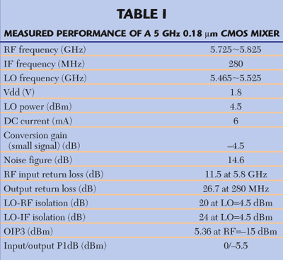
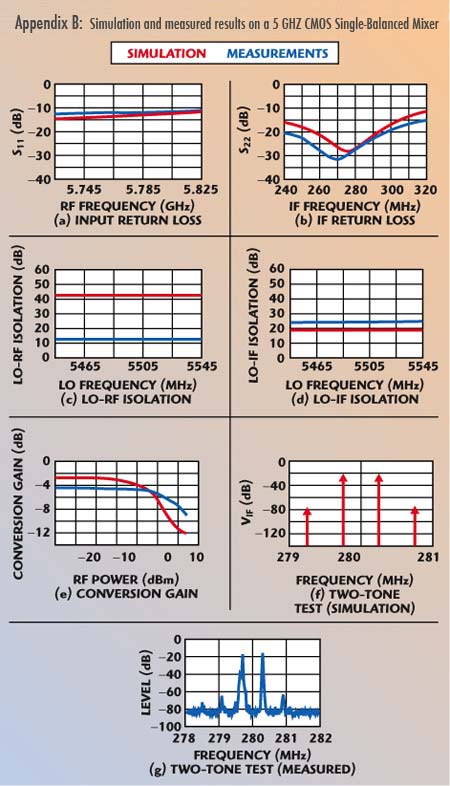
Appendix B shows the simulation and measurement results of a 5 GHz CMOS single-balanced mixer. The measured conversion gain is 5.5 dB at the input P1dB of 0 dBm. With a noise figure of 14.6 dB and an OIP3 of 5.36 dBm, the LO-to-RF and LO-to-IF isolations are 20 and 24 dB, respectively. The measurements basically agree with the simulation results except for the LO-to-RF isolation. It may be due to the substrate coupling of the LO and RF ports or the process variation causing an asymmetry between M2 and M3 (and hence an LO unbalance). The LO-RF isolation could be improved by shielding the pads with guard rings. The power consumption is 10.8 mW at VDD = 1.8 V. The summary of the measured characteristics of a 5 GHz CMOS single-balanced mixer is shown in Table 1.
 | ||
Conclusion
A 5 GHz CMOS single-balanced mixer, fabricated in a TSMC 0.18 mm standard CMOS process, is presented. For an IEEE 802.11a WLAN application (5.725 to 5.825 GHz), the LO is set at 5445 to 5545 MHz and the IF is 280 MHz. The measurements are performed using a FR-4 PCB test fixture. The fabricated mixer exhibits a small signal conversion gain of –4.5 dB, a noise figure of 14.6 dB, an input P1dB of 0 dBm and an OIP3 of 5.36 dBm. The LO-to-RF and LO-to-IF isolations are 20 and 24 dB, respectively. The power consumption is 10.8 mW at VDD = 1.8 V.
Acknowledgment
The authors would like to thank the Chip Implementation Center (CIC) of the National Science Council, Taiwan, ROC, for its support of the TSMC CMOS process.
 | ||
 | ||
References
-
T.H. Lee, The Design of CMOS Radio-frequency Integrated Circuits, Cambridge University Press, New York, NY 1998.
-
IEEE Std 802.11a/D7.0-1999, “Part 1: Wireless LAN Medium Access Control (MAC) and Physical Layer (PHY) Specifications: High Speed Physical Layer in the 5 GHz Band.”
-
B. Razavi, RF Microelectronics, Prentice Hall, 1997.
-
J. Maligeorgos and J. Long, “A Low Voltage 5.1-5.8 GHz Image-reject Receiver with Wide Dynamic Range,” IEEE Journal of Solid-State Circuits, Vol. 35, No. 12, December 2000, pp. 1917–1926.
Yuan-Kai Chu received his MSEE degree from National Cheng Kung University, Tainan, Taiwan, in 2002, where he worked on 5 GHz CMOS RFICs for his master study. He is currently with the HiMAX Opto-electronics Corp. as an R&D engineer. His research interests include RFIC/MMIC design for wireless communication systems.
Huey-Ru Chuang received his BSEE and MSEE degrees from National Taiwan University, Taipei, Taiwan, in 1977 and 1980, respectively, and his PhD degree in electrical engineering from Michigan State University, East Lansing, MI, in 1987. From 1987 to 1988, he was a post-doctoral research associate at the Engineering Research Center, Michigan State University. From 1988 to 1990, he was with the Portable Communication Division of Motorola Inc., Ft. Lauderdale, FL. He joined the department of electrical engineering at National Cheng Kung University, Tainan, Taiwan, in 1991, where he is currently a professor. His research interests include antenna and RFIC/microwave circuits design for wireless communications, computational electromagnetics and applications, EMI/EMC, microwave communication and detection systems.