
Under exacting demands from customers, wireless systems providers are developing integration solutions to reduce the size, power consumption and cost of their systems. The trend now is that many of the non-semiconductor devices will be replaced by either software radio algorithms,1 or by miniature passive devices fabricated using silicon-based MEMS technologies.2
 | |||
| Fig. 1 Test set-up for a one-port clamped-clamped micromechanical resonator. | |||
Many of the non-semiconductor devices are made of crystals such as quartz and lithium niobate,3 which means they have to be connected to RFICs at the board level. These devices are implemented in wireless systems mainly for signal processing and frequency selection. Since their operation is mechanical, they also exhibit excellent Qs (Q>10,000). Integrated circuits, on the other hand, are only able to provide Qs under 75.4 Fundamentally, the size of these mechanical devices is large, and they cannot be integrated into planar silicon processes at this time.
Previous work, performed at the University of Michigan, demonstrated Qs of 4000 for 10 MHz clamped-clamped beam polysilicon micromechanical resonators5 that vibrate vertically to the substrate surface. The input signal for this type of resonator is applied on the electrode under the resonator, while both the DC-bias voltage and output signal are connected onto the resonator, as shown in Figure 1. A bias-tee is required to separate the DC-bias voltage and the RF signal. However, a bias-tee is not practical for integration of these devices into a planar process.
Therefore, the objective of this work is to demonstrate the design for a 10 MHz polysilicon micromechanical resonator with a Q greater than 10,000 for reference oscillator applications. Resonators with two separate electrodes will be demonstrated to eliminate the bias-tee, which decreases the feedthrough capacitance of the device.
Initial Design Consideration for RF MEMS Resonators
 | |||
| Fig. 2 Motional resistance vs. gap spacing between electrode and resonator. | |||
To maximize the Q of the resonator, free-free (FF) beam resonators6 are required, since the anchor dissipation of this type of resonator is optimized using quarter wavelength suspension beams. Previous work on FF-beams that vibrate vertically to the substrate surface demonstrated a Q of 8110 at 31.51 MHz. However, at 10 MHz, the quarter wavelength suspension beams become 94 ![]() m long and 1
m long and 1 ![]() m wide. Therefore, the resonator beam could be catastrophically pulled-in when 1 V of DC-bias voltage is applied. Although dimples could prevent the beam from being pulled-in, this type of resonator still yields reliability issues, making it unsuitable for most wireless applications.
m wide. Therefore, the resonator beam could be catastrophically pulled-in when 1 V of DC-bias voltage is applied. Although dimples could prevent the beam from being pulled-in, this type of resonator still yields reliability issues, making it unsuitable for most wireless applications.
Therefore, the next option considered is the lateral resonator. If the motional resistance were not an issue for oscillator circuits, implementing this option could be as easy as laying out a lateral FF-beam with optimized supports. As shown in Figure 2, the plot of motional resistance versus the gap spacing between the electrode and the resonator illustrates that when using a 1![]() m gap spacing, which is the lithography limit of a four inch contact aligner, the motional resistance is greater than 10 M
m gap spacing, which is the lithography limit of a four inch contact aligner, the motional resistance is greater than 10 M![]() . This level of motional resistance makes an oscillator design nearly impossible. A new process that provides submicron capacitive gaps is required if the 1 mm lithography limit remains in effect. Therefore, a new foundry process must be developed to allow this device to be fabricated.
. This level of motional resistance makes an oscillator design nearly impossible. A new process that provides submicron capacitive gaps is required if the 1 mm lithography limit remains in effect. Therefore, a new foundry process must be developed to allow this device to be fabricated.
 | |||
| Fig. 3 Test set-up for a two-port lateral free-free micromechanical resonator. | |||
Figure 3 shows a schematic of the lateral FF-beam resonator in a typical measurement circuit. This resonator consists of an FF-beam suspended at its nodal locations by four flexural support beams. The resonance frequency of the FF-beam is given by
where
E = Young’s modulus
![]() = density
= density
Lr = length of the resonator beam
Wr = width of the resonator beam
To suppress energy losses from the FF-beam to the support anchors, the support beams and FF-beam are joined at the two nodal points of the FF-beam. The length of the support beam is designed so that the support beams on opposite sides of the FF-beam (from anchor-to-anchor) resonate in a second mode with respect to the fundamental mode frequency of the FF-beam. With this design, the beam attachment locations correspond to nodal points for both the composite support beams and the FF-beam resonator, creating a high (ideally infinite) impedance location through which very little energy is transferred, hence, through which very little energy is dissipated. The length of the support beam is given by
where
Ls = length of the support beam
Ws = width of the support beam.
Process Considerations for Fabricating Resonators
 | |||
| Fig. 4 Electrode structure options; | |||
The plot of motional resistance versus gap spacing shows that the spacing between the resonator and electrode must be less than 1000 Å for better electromechanical coupling. However, it is difficult and not cost effective to achieve uniform 1000 Å wide, 2 ![]() m deep air gaps using e-beam or deep-submicron lithography tools or reactive ion etching (RIE) facilities. Therefore, a new low cost process is required for fabricating this assembly.
m deep air gaps using e-beam or deep-submicron lithography tools or reactive ion etching (RIE) facilities. Therefore, a new low cost process is required for fabricating this assembly.
To form such a small air gap, the best way to define the gap spacing is to control the thickness of the sacrificial oxide. To achieve this, resonator structures are RIE etched first, and then the sacrificial layer is conformally deposited around the resonator structure, assuming the equal thickness of sacrificial layer on the sidewall and on the top of the resonators.
Next, the electrodes for this structure can be designed, although there are options to consider, as shown in Figure 4. The metal may be plated only against the sidewall but not on top of the resonators or another layer of polysilicon can be deposited and the polysilicon on top of the resonator then polished off. After analyzing the cost of this procedure, the metal electrode was determined to provide a lower cost with a faster turn-around time in fabrication.
Hence, the requirements for successfully fabricating the metal electrodes are that they can be plated, not etched by HF, and provide good adhesion to the substrate during the HF release. After some research on material properties, gold (Au) and palladium (Pd) were found to be good candidates for the electrodes. Gold was ultimately selected since it was readily available from plating facilities.
Next, a process is required to ensure that gold is not plated on top of the resonators. Since electroplating only happens on the regions where there is a seed layer and the seed layer is exposed to the plating solution, the question was whether it would be possible to place photoresist exactly on top of the resonator structure. The problem was that one slight misalignment would destroy the device. This is resolved by removing the seed layer on top of the resonator, and keeping the seed layers on the resonator sidewalls.
The other process to prevent Au from being plated on top of the resonator is to spin on thick photoresist and then etch-back the photoresist. Thick photoresist can be spun on the wafer to yield a flat surface. The photoresist is then etched in an O2 plasma until the top surface of the resonators is exposed. At this time, since the other part of the seed layer is still covered by photoresist, the top seed layer can be removed by wet etching. With no seed layer on top, the Au electrode is selectively plated between the sidewall of the resonator and the photoresist plating mold.
 | |||
| Fig. 5 Simulated displacement contour plot of a lateral FF-beam micromechanical resonator. | |||
The proof-of-concept fabrication for this device was performed in the Solid-state Electronics Laboratory at the University of Michigan. The material properties of polysilicon were characterized for this facility by previous researchers,7 allowing the resonator frequency to fall into the specified target range. Frequency variations of five percent are typically experienced due to lithography variations and thin film uniformity issues. Accurately knowing the material properties for this foundry proved to be a critical step for designing this device. This is particularly true if the device is required to satisfy the performance objectives using only one foundry run.
Design Verification
The fundamental question in the verification phase of this program is to determine the resonant frequency of the structure as it will be fabricated. The mode shape of the lateral FF-beam resonator employing the second-mode supporting beam structure was simulated using ANSYS Multiphysics.8 The results shown in Figure 5 demonstrate a displacement contour plot that verifies the mode shape of the beam and supports, and demonstrates the lack of displacement at the nodal locations. The material properties were obtained from prior material characterizations for the fabrication facility. This allowed the resonant frequency for the resonator to be exactly 10 MHz in this design verification simulation. Therefore, the design does not need to be manipulated to achieve the resonant frequency specification for the resonator. The device may now be fabricated to experimentally verify the performance of the resonator.
Resonator Fabrication
The fabrication process begins with steps similar to those used in polysilicon surface micromachining, then continues with the conformal deposition of 1000 Å of high temperature oxide (HTO) along the tops and sidewalls of the patterned polysilicon structures to serve as a sacrificial layer that defines the eventual electrode-to-structure capacitive gap spacing. At this point in the process, the device cross-section is shown in Figure 6(a). The bottom 6000 Å sacrificial oxide is then patterned and etched to expose the underlying nitride film (without attacking it) in areas where metal electrodes are to be formed.
 | ||
| Fig. 6 Process flow for lateral FF-beam micromechanical resonators. | ||
In preparation for metal electroplating, a thin Cr/Au/Cr (200 Å/300 Å/200 Å) film is evaporated over all areas to provide a seed layer, as shown in Figure 6(b). Next, a 14 mm-thick layer of SJR5740 photoresist (PR) is spun onto the wafer — thick enough to achieve a planarized surface, with the structural polysilicon topography deep under the PR film. The PR is then etched back using an O2 plasma process until the seed layer over the top of the polysilicon structures is exposed. The exposed top-level seed layer is then removed using a combination of Cr and Au etching solution to prevent metal from plating over the top of the polysilicon structures during subsequent electrode plating steps. At this point in the process, the cross-section for the device is shown in Figure 6(c). After removing the remaining film of the SJR5740 photoresist, a 6 ![]() m-thick AZ9245 photoresist layer is applied and patterned to the electrode geometrical specifications to form a mold that, together with the sidewall sacrificial oxide, defines the electrode plating boundaries.
m-thick AZ9245 photoresist layer is applied and patterned to the electrode geometrical specifications to form a mold that, together with the sidewall sacrificial oxide, defines the electrode plating boundaries.
 | |||
| Fig. 7 Electrode-to-structure gap spacing as fabricated. | |||
 | |||
| Fig. 8 SEM photograph of the fabricated lateral FF-beam micromechanical resonator with Au electrodes. | |||
After removing the top Cr layer to expose the Au seed layer (using the mold as a mask), Au is electroplated to form the electrodes and achieve the cross-section shown in Figure 6(d). Au is plated until the electrode top is nearly flush with the top of the polysilicon structure, as shown in Figure 6(e). Note that the 3000 Å oxide on top of the polysilicon structures (originally used as a hard mask during poly etching) provides a buffer zone over which the electrode metal can be plated beyond the polysilicon thickness while avoiding plating over the top of the polysilicon structures. After plating, the photoresist mold is removed, and a thin layer of Ni is plated over the exposed Au electrode regions (with Cr blocking any plating in field regions) to protect them during a subsequent seed layer removal step.
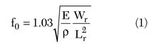
After seed layer removal, the structures are released in 49 percent concentrated HF to yield the final cross-section shown in Figure 6(f). During the typical 10-minute HF dip required to release all of the structures, the adhesion between the Au electrodes and the nitride isolation layer remains intact. The electrode-to-structure gap spacing is 1013 Å for this process run, as shown in Figure 7, which provides an aspect ratio of about 30 for the 3 ![]() m-thick structures shown here. Note that the aspect ratio is limited only by the conformability of HTO and the maximum thickness to which Au can be plated. Finally, Figure 8 shows the SEM photograph of the fabricated lateral FF-beam micromechanical resonator with Au electrodes.
m-thick structures shown here. Note that the aspect ratio is limited only by the conformability of HTO and the maximum thickness to which Au can be plated. Finally, Figure 8 shows the SEM photograph of the fabricated lateral FF-beam micromechanical resonator with Au electrodes.
Resonator Test Results
As shown in Figure 9, the Q of a lateral free-free beam resonator is 10,743 at 10.47 MHz. This frequency can be tuned to exactly 10 MHz by adjusting the DC-bias voltage. Therefore, both specifications for the resonator have been successfully met. Please notice that the low amplitude of the spectrum is caused by the impedance mismatch between the motional resistance and the 50 ![]() termination provided by the network analyzer.
termination provided by the network analyzer.
 | ||
| Fig. 9 Measured frequency spectrum of the lateral FF-beam micromechanical resonator. | ||
This process can also be used for fabricating disk resonators. Initial results from disk resonators demonstrated a Q of 9400 at 156 MHz, as shown in Figure 10. It is possible to make micromechanical resonators operating above 1 GHz for filter applications by shrinking the diameter of the disk.
 | ||
| Fig. 10 Disk resonators demonstrating a Q-factor of 9400 at 156 MHz. | ||
Conclusion
A design procedure has been described for a lateral free-free micromechanical RF MEMS resonator. This resonator was fabricated using the surface micromachining procedure developed and demonstrated by Discera Inc. Test results for 10 MHz resonators fabricated using this new process have demonstrated Qs in excess of 10,000 with a maximum frequency variation of five percent across the diameter of a wafer. Frequency variations of this type are compensated for with DC-biasing of the resonator.
Therefore, the device development community has been provided with sufficient design and process information to allow these devices to begin displacing crystals for reference oscillator applications. Applications for these devices will grow as this technology matures.