
The reliability of GaAs power FETs used in solid-state power amplifiers (SSPA) is adversely affected when operated in an overdrive (excess input power) condition for a long time due to excess gate current. Manufacturers of SSPAs use different schemes to protect the FET power devices from overdrive conditions. One method is to distribute the compression in the device chain; another is to use a limiter circuit. In both cases, however, it is very difficult to fully protect the devices from an overdrive condition, which becomes worse when the SSPAs operate in a varying temperature environment. Some manufacturers also use a feedback control loop for this purpose but its limiting power level is highly sensitive to temperature. A temperature-compensated closed loop overdrive control circuit can eliminate these problems.
In this article a detailed description (with mathematical expressions and test results) of a temperature-compensated closed loop overdrive level control (OLC) circuit is presented. This scheme can properly protect the FET power devices from overdrive conditions, irrespective of the change in temperature, and the described mathematical expressions help to design the temperature compensation network without trial and error.
A Different OLC Scheme
Manufacturers of SSPAs use different schemes to protect the GaAs power FET devices from overdrive conditions. In some cases, a proper device chain is selected to distribute the overdrive power among the devices in the SSPA so that the power devices cannot be heavily compressed and the gate current of the GaAs FETs remain within the appropriate limit. However, in this case, the device selection in the line up is not simple. Also, precise overdrive protection of the devices is not possible without compromising the nonlinearity of the SSPAs, which becomes worse when the SSPAs operate in varying temperature environments.
Another approach to protect the FET devices from overdrive power is the use of Schottky barrier diode (SBD)-based or GaAs FET-based limiters1,2 at microwave frequencies. However, these limiters can operate only at low power levels. Therefore, the gain variation over temperature of the intermediate stages used between the power device and the limiter circuit will change the limiting power level. Thus, in practice, limiter circuits are not suitable to properly protect the FET power devices used in SSPAs under overdrive conditions.
Some SSPA manufacturers use closed loop power control systems for this purpose. But, due to the high closed loop gain, the limiting power level is very sensitive to the variation of the detector diodes’ behavior over temperature. A temperature-compensated closed loop overdrive control circuit can eliminate all of these disadvantages.
Closed Loop OLC Operation
A simplified schematic block diagram of a closed loop overdrive level control system is shown in Figure 1. This scheme is capable of protecting the high power FET devices in the power amplifier as well as the small signal and medium power FET devices in the driver amplifier from overdrive conditions. Since a power sampler is used to sample and detect the power level, this scheme can be used to control any level of high power output.
 | ||
| Fig. 1 Block diagram of an overdrive level control loop. | ||
At microwave frequencies Schottky diode detectors are mainly used to detect power. A control voltage VC is applied to the detector diode to finely adjust the limiting power level. There will be a detected voltage when the coupled power exceeds a certain specified level determined by the barrier potential (![]() ) of the Schottky barrier diode and the given control bias VC. This detected voltage is amplified by a DC amplifier and fed to a voltage-controlled attenuator. PIN diode-based attenuators are commonly used as voltage-controlled attenuators. Depending upon the required amount of overdrive level protection, single- or multi-stage attenuators are used.
) of the Schottky barrier diode and the given control bias VC. This detected voltage is amplified by a DC amplifier and fed to a voltage-controlled attenuator. PIN diode-based attenuators are commonly used as voltage-controlled attenuators. Depending upon the required amount of overdrive level protection, single- or multi-stage attenuators are used.
The test response of a closed loop OLC is shown in Figure 2, where Pi_N and Po_N are the normalized input and output power. Here, different limiting power level settings are achieved by controlling the bias voltage (VC) of the Schottky barrier diode.
 | ||
| Fig. 2 Closed loop OLC response under different control bias voltages. | ||
Temperature Behavior of a Closed Loop OLC
The behavior of the PIN diode attenuator and driver amplifier circuit in the OLC system changes with temperature. The RF resistance of the PIN diode in the attenuator circuit changes with temperature, causing a variation in attenuation of the PIN diode attenuator. The gain of the FET devices used in the driver amplifier circuit also changes with temperature. Due to the variation of the attenuation of the attenuator and the gain of the driver amplifier, the power at the input of the detector will vary.
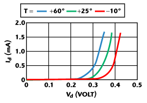 | ||
| Fig. 3 I-V characteristics of Schottky barrier diode over temperature. | ||
In addition, the I-V characteristics of the detector diode change with temperature, as shown in Figure 3. In the case of hard limitation of the power level, the gain of the DC amplifier is very high. Therefore, a small change of the detector diode voltage causes a significant change of the limiting power level. The test results of the limiting variation of limiting power level of the OLC system, due to the temperature variation of only the detector diode, are shown in Figure 4. The limiting power level variation is observed to be approximately 3 dB peak-to-peak for a temperature variation of –10° to +60°C.
 | ||
| Fig. 4 OLC response due to the variation of temperature of the detector diode. | ||
Closed Loop OLC Temperature Compensation
The changes in limiting power level due to the attenuation variation of the attenuator and the gain variation of the driver amplifier are eliminated inherently due to the closed loop negative feedback behavior of the OLC system. Since the gain of the DC amplifier is very high, when the power level at the detector input changes due to the temperature variations, the detector output changes automatically to adjust the attenuation of the attenuator to keep the input at the detector constant.
Therefore, as long as the detector diode behavior is unchanged, any power variation at the input of the detector will be compensated by automatically changing the detected output voltage, which adjusts the attenuation level such that the power level at the input of the detector remains constant. Thus, attenuation and gain variation of the attenuator and FET devices of the driver amplifiers, respectively, will not affect the limiting power level of the OLC circuit if the voltage variation of the detector diode can be compensated over the temperature range of interest.
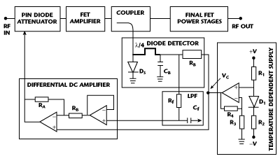
A temperature-compensated OLC scheme is shown in Figure 5. The temperature dependent control voltage VC biases the detector diode DS through a bias network containing a resistor RB and an RF decoupling network containing a ![]() /4 transmission line and a capacitor CB.
/4 transmission line and a capacitor CB.
 | ||
| Fig. 5 Schematic circuit diagram of a temperature-compensated closed loop OLC. | ||
The output of the detector diode, filtered by a low pass filter, is then connected to one input of the differential DC amplifier. The other input is connected to the control voltage VC. The output of the differential amplifier is connected to the control terminal of the PIN diode attenuator circuit.
When the RF power is below the limiting power level (threshold power level) there is no detector diode current. Therefore, the voltages at the two inputs of the differential amplifier are the same; the output voltage is zero and there is no change in attenuation of the attenuator. When the RF power amplitude exceeds the threshold power level, the detector diode starts to conduct. Therefore, there will be a voltage difference between the inputs of the differential amplifier, which leads to a finite output voltage at the output of the differential amplifier. This output voltage sets the attenuation of the attenuator so that the RF power will be limited to the predetermined limiting power level. Changing the control voltage VC to the diode can compensate for the variation of limiting power level due to the variation of detector diodes voltage Vsbd over the temperature. To achieve this, the combination of the detector diode voltage and control voltage, that is Vsbd-VC, should remain invariant over the temperature range of interest. Therefore, the condition for temperature compensation is

The I-V characteristics over the temperature, for a P-N junction diode and a Schottky barrier diode, are similar in nature. Therefore, a temperature dependent voltage source VC is generated by using the temperature dependent voltage drop of a P-N junction diode D1.
In the circuit shown, the control voltage VC is given by
where
G = 1 + R4/R3
r = R2/R1
Vpnd = voltage across the P-N junction diode D1
Therefore, by combining Equations 1 and 2, the condition for compensation becomes

Now the temperature dependent I-V relationship of the diode is given by3
where
Vd = diode voltage
A = area factor of the diode, independent on temperature
![]() = diodes ideality factor
= diodes ideality factor
Eg = band gap potential of the semiconductor in the case of a P-N junction diode and the barrier potential (![]() ) in the case of a Schottky barrier diode
) in the case of a Schottky barrier diode
m = temperature exponent of the diode
k = Boltzman’s constant
q = electron charge
The load line equation is given by
![]()
where
Vd = diode voltage at current Id when biased by a voltage source Vs through a vias resistor Rb
For a forward biased diode, where the reverse saturation current is negligible compared to the total forward current, the rate of change of the diode voltage with respect to the temperature is given by Equations 4 and 5

where
VT = kT/q
Equation 6 is valid for both P-N junction and Schottky barrier diodes. Thus, knowing the diode parameters present in Equation 6, the circuit component values for the temperature dependent voltage source can be derived from Equations 2, 3 and 6.
Circuit Realization and Test Result
The schematic circuit shown has been implemented for a C-band solid-state power amplifier. The voltage-controlled attenuator, using an HPND 4005 PIN diode, has been realized on an alumina substrate (![]() r = 9.9) by using a 3 dB Lange coupler in a microstrip line configuration. The power sampler and detector circuits, using an HSCH 5315 Schottky barrier diode, are also realized on an alumina substrate. To generate the temperature dependent control voltage, a 1N5806 P-N junction diode is used with a supply voltage of ±5 V. The high gain differential DC amplifier uses the µA741 operational amplifier.
r = 9.9) by using a 3 dB Lange coupler in a microstrip line configuration. The power sampler and detector circuits, using an HSCH 5315 Schottky barrier diode, are also realized on an alumina substrate. To generate the temperature dependent control voltage, a 1N5806 P-N junction diode is used with a supply voltage of ±5 V. The high gain differential DC amplifier uses the µA741 operational amplifier.
Typical parameters for the HSCH-5315 Schottky barrier diode are Eg = 0.69 V, ![]() = 1.1, m = 3 and Vsbd = 0.28 V. The detector diode operates under very high bias resistor; therefore,
= 1.1, m = 3 and Vsbd = 0.28 V. The detector diode operates under very high bias resistor; therefore, ![]() VT <dRb. From these values, dVsbd/dT is found to be 1.6 mV/°C at room temperature. Typical parameters for the 1N-5806 P-N junction diode are Eg=1.16 V,
VT <dRb. From these values, dVsbd/dT is found to be 1.6 mV/°C at room temperature. Typical parameters for the 1N-5806 P-N junction diode are Eg=1.16 V, ![]() =1.5, m=1.5 and Vpnd=0.6 V. Therefore, dVpnd/dT = 2.1 mV/°C at room temperature. Introducing these values in Equations 2 and 3, and considering the P-N junction diode to operate at a current of 10 mA, and the control voltage (VC) requirement at room temperature being 0 V, the circuit parameters become R1 = 500Ω, R2=440Ω, R3=1 kΩ and R4=433Ω.
=1.5, m=1.5 and Vpnd=0.6 V. Therefore, dVpnd/dT = 2.1 mV/°C at room temperature. Introducing these values in Equations 2 and 3, and considering the P-N junction diode to operate at a current of 10 mA, and the control voltage (VC) requirement at room temperature being 0 V, the circuit parameters become R1 = 500Ω, R2=440Ω, R3=1 kΩ and R4=433Ω.
The test results of the temperature-compensated OLC circuit are shown in Figure 6. It is clear that the limiting power level remains nearly invariant over the temperature range of –10° to +60°C.
 | ||
| Fig. 6 Complete OLC circuit response over the temperature variation. | ||
Conclusion
The temperature-compensated closed loop control circuit scheme presented here can be used not only for SSPAs but also in any microwave system for power level control. These types of microwave power limiters are also suitable in signal processing, for example, to suppress AM components before demodulation of a microwave FM signal, since a PIN diode attenuator offers very low phase variation over the attenuation range.
Acknowledgment
The authors would like to express their gratitude to Shri V.K. Garg, deputy director, Satcom-Payload Technology Area, SAC, for his encouragement and support of this work.
References
- T. Para, et al., “Design of a Low Phase Distortion GaAs FET Power Limiter,” IEEE Transactions on Microwave Theory and Techniques, Vol. 39, June 1991, pp. 1059–1062.
- T. Para, et al., “X-band Low Phase Distortion MMIC Power Limiter,” IEEE Transactions on Microwave Theory and Techniques, Vol. 41, May 1993, pp. 876–879.
- S.M. Sze, Physics of Semiconductor Devices, Second Edition, Willy Eastern Ltd.
S.C. Bera received his M.Tech. degree in radio physics and electronics from the University of Calcutta, and joined the Indian Space Research Organization, Ahmedabad Centre, in 1994. Since joining ISRO, he has been involved in many payload projects, including the INSAT-2C, 2E, INSAT-3A, 3E and GSAT series of spacecrafts. He is presently deputy project manager for SSPAs for the INSAT-3E and SATNAV payload projects. His interests include the design and development of SSPAs, channel amplifiers, linearizers, attenuators and phase shifters.
R.V. Singh received his B.Tech (EE) degree from the GB Pant University of AG and Technology, Pantnagar, Nainital, in 1972. He joined the Experimental Satellite Communication Earth Station (ESCES), Ahmedabad, India, in October 1972, which later became a part of the Space Applications Centre (ISRO). He was the associate project director for INSAT-3A communication payload, and is presently working as group director of the Power Amplifier Group in the SATCOM payload technology area of the Indian Space Research Organization. His interests include microwave low noise amplifiers and receivers for communication satellite transponders.