
Microwave oscillators form an important part of all microwave systems, such as those used in radar, communication links, navigation and electronic warfare.1 Oscillators are required to have excellent frequency stability against variations in temperature, power supply voltage and oscillator loading (load pulling). They also need a power output adequate for their application, as well as low noise,2–5 especially when many stages of frequency conversion are used and there is the addition of uncorrelated phase noise from the various oscillators. There must be some degree of electrical or mechanical tuning capability. Frequency stability and low noise are obtained by using a high Q resonator in the frequency-determining circuit. Loose coupling to the load allows some immunity against frequency variation with changes in load impedance.
DROs are attractive microwave sources, as fixed or narrowband tunable oscillators. They represent a good compromise between cost, size and performance compared to alternative signal sources such as cavity oscillators, microstrip oscillators or multiplied crystal oscillators. The dielectric resonator (DR), which is the frequency-determining element of the DRO, is a piece of high dielectric constant ceramic material with characteristics similar to a metallic resonant cavity, but much smaller in size.6 The important material properties for DR applications include the temperature coefficient of resonant frequency (![]() f), the unloaded Q factor (QU) and the dielectric constant of the material (
f), the unloaded Q factor (QU) and the dielectric constant of the material (![]() r), which will ultimately determine the resonator dimensions.7 The advantages of substituting the DR for a conventional resonator are smaller physical size, ruggedness, low cost, tunability, capability of oscillation over a large frequency range, and temperature stability if the correct material is used. The DRO can offer low DC supply power requirements, good output power, wide operating temperature range, low phase noise characteristics and good efficiency.6
r), which will ultimately determine the resonator dimensions.7 The advantages of substituting the DR for a conventional resonator are smaller physical size, ruggedness, low cost, tunability, capability of oscillation over a large frequency range, and temperature stability if the correct material is used. The DRO can offer low DC supply power requirements, good output power, wide operating temperature range, low phase noise characteristics and good efficiency.6
This article describes the study of a C-band DRO designed for low phase noise characteristics. The design is based mainly on measurements of the DR at its TE01∂ resonant mode combined with simulation of the remaining circuitry using known models for the transistor. Several CAD tools such as LIBRA,8 Computer Aided Resonator Design (CARD)9 and Microwave Office were used.
Design Theory
The noise figure of the active device is a major factor in the oscillator’s phase noise. Following selection of a suitable low noise device (a type ATF-10136 GaAs FET), the design proceeded in CAD using the measured S-parameters of the resonator and the known S-parameters of the transistor at a recommended DC operating point (Vds = 2 V and Id=25 mA). The circuit was checked for its oscillation condition and optimised for best phase noise and output power. As determined by linear analysis using S-parameters,10 the device is unconditionally stable at the intended operating frequency of 3.65 GHz, and feedback was therefore added. A voltage series feedback at the source was chosen to attain the maximum values for the input and output reflections of the active device at the operating frequency of 3.65 GHz. The linear model with the feedback was optimised using LIBRA software. Figure 1 shows the frequency response of the input and output reflections, where the maximum of both reflections occurs at f = 3.65 GHz, while Figure 2 presents the stability circles but only at the operating frequency of 3.65 GHz. Once the instability region was observed, the output matching circuit was designed for a 50 Ω load.
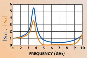 | ||
| Fig. 1 Input and output reflection coefficients of the oscillator circuit as a function of frequency. | ||
 | ||
| Fig. 2 Input and output stability circles of the ATF-10136 device with positive feedback at F = 3.65 GHz. | ||
The type DRD150UC072BU dielectric resonator, provided by Murata, was modeled by Trans-Tech software through their CARD (Computer Aided Resonator Design) program. The DR used has the following properties: diameter (Dr) = 15.02 mm, length (Lr) = 6.66 mm, frequency range is 3.55 to 3.85 GHz, temperature coefficient ![]() f = ±2 ppm/°C,
f = ±2 ppm/°C, ![]() r = 37.4 and minimum Qu = 6000. The DR model was optimised to obtain a reasonable coupling coefficient ß and Q factor at a 3.65 GHz operating frequency. The DR is modeled as a parallel resistor-inductor-capacitor where the values of the inductance L, capacitance C and resistance R are adjusted to provide the proper resonant frequency of 3.65 GHz and Q factor. The coupling with the DR was provided by using a 50 Ω microstrip line on a RT/Duroid substrate of dielectric constant
r = 37.4 and minimum Qu = 6000. The DR model was optimised to obtain a reasonable coupling coefficient ß and Q factor at a 3.65 GHz operating frequency. The DR is modeled as a parallel resistor-inductor-capacitor where the values of the inductance L, capacitance C and resistance R are adjusted to provide the proper resonant frequency of 3.65 GHz and Q factor. The coupling with the DR was provided by using a 50 Ω microstrip line on a RT/Duroid substrate of dielectric constant ![]() r = 2.33, thickness T = 0.79 mm and tan ∂ = 0.0012. The optimum height between the dielectric resonator and the substrate was provided by a dielectric spacer and the DR performance was optimised for both ß and Q. Two types of spacers were tested. The first has a height of 0.79 mm and
r = 2.33, thickness T = 0.79 mm and tan ∂ = 0.0012. The optimum height between the dielectric resonator and the substrate was provided by a dielectric spacer and the DR performance was optimised for both ß and Q. Two types of spacers were tested. The first has a height of 0.79 mm and ![]() r = 2.33, the second a height of 1.5 mm and
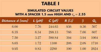
r = 2.33, the second a height of 1.5 mm and ![]() r = 2.55. A low dielectric constant was used for the spacer so that it does not become an electric extension of the dielectric resonator. However, it was found that the best quality factor was obtained when the distance between the DR and the microstrip line was 8.65 mm with the 1.5 mm high spacer. The simulated position of the resonator relative to the line to which it couples was found to be approximately a quarter wavelength for the 1.5 mm high spacer for reasonable values of Q = 1724 and ß = 2.08. The equivalent elements of the DR and the reflection and transmission coefficients are given in Table 1 and Figure 3, respectively.
r = 2.55. A low dielectric constant was used for the spacer so that it does not become an electric extension of the dielectric resonator. However, it was found that the best quality factor was obtained when the distance between the DR and the microstrip line was 8.65 mm with the 1.5 mm high spacer. The simulated position of the resonator relative to the line to which it couples was found to be approximately a quarter wavelength for the 1.5 mm high spacer for reasonable values of Q = 1724 and ß = 2.08. The equivalent elements of the DR and the reflection and transmission coefficients are given in Table 1 and Figure 3, respectively.
 | ||
 | ||
| Fig. 3 Simulated input and output of the dielectric resonator. | ||
Once the DR and its position were modeled, a linear simulation (see Figure 4) was carried out. The linear simulation was checking the condition for oscillation to start, and the predicted oscillation frequency was found to be 3.65 GHz. After tuning the matching circuit and determining the proper resonator model, the nonlinear model can be substituted for the S2P file and used to simulate and optimize the phase noise and power performance of the circuit. However, the complete model of the biasing network needs to be included at this point to obtain accurate predictions. The transistor was biased via two quarter-wave transmission lines, each having a radial stub at one end to create an effective RF short circuit that is transformed to an infinite impedance at the transistor connection. The width of the quarter wavelength line should be made as narrow as possible to maintain the highest impedance over the working bandwidth, and was selected to be 0.3 mm for reliable PCB manufacturing.
 | ||
| Fig. 4 Model for the linear analysis of the DRO. | ||
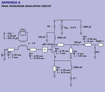
The final circuit schematic for the DRO, used in nonlinear simulation, is shown in Appendix A, whereas the final oscillator circuit model is given in Appendix B. The final nonlinear model was tested and optimised to meet the target specifications and to predict the single-sideband noise, phase spectrum and harmonics levels over the band of interest.
Simulation and Measurement Results
After achieving satisfactory results in simulation and choosing the appropriate circuit components, a prototype board was constructed and tested for compliance with the proposed specifications. It is shown in Figure 5. After some adjusting of the output matching parallel stub, the oscillator yielded the expected TE01∂ resonant mode with output power of 11.7 dBm. It was also verified that the oscillator would not have spurious oscillations at undesired frequencies by removing the DR. Once basic oscillation conditions were attained, the phase noise performance was investigated and the DR placement optimized.
 | ||
| Fig. 5 Prototype of the DRO. | ||
The DR was first moved along the transmission line to optimize the output power, fairly close to the line (to provide a strong coupling). Once this reference plane was located, the spacing between the DR and the line was varied in order to increase the loaded Q of the DRO and improve phase noise. The compromise is that the spacing must be large enough to minimise the phase noise, and small enough to obtain an acceptable output power and reliable starting of the oscillator. When this was optimized, the design was able to provide an adequate tuning range with a limited power variation. Changing the termination at the input of the transistor caused the harmonics to decrease by 6 dB because the chip resistor used departed substantially from ideal behaviour at the higher frequencies.
 | ||
| Fig. 6 Output spectrum of the free-running DRO. | ||
The free running frequency without the tuner was observed at 3.577872 GHz. A minimum of 11.5 dBm output power was achieved. The phase noise at 100 kHz offset was found to be –120 dBc/Hz. Figure 6 shows the measured output power and phase noise performance that was achieved. The measured efficiency was 10.8 percent. The fine tuning and adjustment of the DRO can be set through a tuning screw that will increase the DR’s resonant frequency as it displaces the electrical field above the DR. Figure 7 shows the maximum tuned measured resonance frequency of the DRO at 3.7 GHz with 12.5 dBm output power. In general, a tuning range of 130 MHz was achieved without degrading the output power or the phase noise performance. The output spectrum harmonics of the oscillator is shown in Figure 8. As can be seen on the graph, a second harmonic rejection of 22.7 dB was observed, and no other spurious of any kind was observed above –120 dBc. The frequency pulling and the external quality factor were found to be 900 and 1930 kHz, respectively, whereas the frequency pushing for a maximum of 1 V was 125 kHz, that is approximately 0.0034 percent of the measured oscillation frequency.
 | ||
| Fig. 7 Output spectrum of the DRO tuned to its maximum frequency. | ||
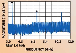 | ||
| Fig. 8 Measured output harmonic levels | ||
Conclusion
A simple approach for designing a reflection-stabilized oscillator with a dielectric resonator placed at the input was described. The required performance specifications were presented. A simple set of design rules for a reflection-stabilized DRO was presented. Conditions for low phase noise were then discussed. It was shown that a low phase noise oscillator is dependent upon the choice of the active device, its operating point, the supporting circuit components and the unloaded quality factor of the resonator.
Complete characteristics of the DR were simulated using CARD, then measured using a network analyzer. It was shown that placing the DR on a spacer resulted in better performance than placing it directly on substrate. Practical realization and measured results were then discussed. The result was that all the specification goals were met. In general, the design of any DRO requires tradeoffs between phase noise, output power, tuning range and frequency stability.
References
- D. Kajfez and P. Guillon, Dielectric Resonators, First Edition, Artech House Inc., Norwood, MA, 1986.
- C.D. Prasad, S.S. Sarin and D. Singh, “Low Phase Noise GaAs Gunn Dielectric Resonator Oscillator at Ka-band,” IETE Technical Review, Vol. 17, Nos. 1-2, January–April 2000, pp. 67–70.
- O. Bernard and R. Croston, “Simulate and Build a Ku-band DRO,” Microwaves and RF, Vol. 39, No. 5, May 2000, p. 103.
- C. Tsironis, “Highly Stable Dielectric Resonator FET Oscillators,” IEEE Transactions on Microwave Theory and Techniques, Vol. 33, No. 4, April 1985, pp. 310–314.
- R. Muat, “Low Noise Oscillator Design: Choosing Devices for Quiet Oscillators,” Microwaves and RF, Vol. 23, No. 8, August 1984, p. 166.
- L.A. Tringogga, G. Kaizhou and I.C. Hunter, Practical Microstrip Circuit Design, First Edition, Ellis Horwood Ltd., 1991.
- A. Khanna and Y. Garault, “Determination of Loaded, Unloaded Factors of a Dielectric Resonator Coupled to a Microstrip Line,” IEEE Transactions on Microwave Theory and Techniques, Vol. 31, No. 3, March 1983, pp. 261–264.
- Agilent Corp., “RF Momentum Software and Circuit Simulator,” Libra Package Series IV.
- Trans-Tech Inc., “Introduction to Dielectric Resonators,” Application Notes 1030, 851 and 821, http://www.trans-techinc. com/TTapnote.cfm.
- G. Vendelin, R. Pavio and V. Rohde, Microwave Circuit Design Using Linear and Nonlinear Techniques, Wiley-Interscience, 1990.
 | ||
 | ||