
 | |||
Modern wireless transmitters generally incorporate circuitry that directly or indirectly measures and regulates transmitted power. There are a number of reasons for this. Cellular standards such as WCDMA, CDMA2000 and GSM/EDGE demand that both base station and handset power be tightly controlled so that spectral leakage into adjacent channels and in-band blocking scenarios are kept below a defined minimum. Measurement of a base station’s (BTS) maximum output power is also required to minimize excess thermal dimensioning (heat sinks) and to provide an alarm output if the power amplifier starts transmitting too much power or if the antenna is damaged. Similar requirements exist in applications that use spectrum beyond 2 GHz (point-to-point, point-to-multipoint links, WLAN and radar, for example).
While wireless standards typically call for a transmitted power precision of between ±1 and ±2 dB, there are clear advantages associated with going beyond these requirements. Setting the transmitted power as close as possible to that demanded by the system reduces current consumption, keeping down utility bills in large cell sites. In addition, active power amplifier linearization algorithms will have to work harder to reduce distortion if the transmitted power is 2 dB higher than it needs to be.
Power detection has traditionally been implemented using a simple diode detector circuit. In recent years, demodulating log amplifiers have begun to replace diode detectors because of their ease of use and their much larger detection range (typically 45 to 100 dB vs. 20 to 35 dB for a finely tuned diode detector). While diode detectors have excellent temperature stability at high input powers (for example, +15 dBm), even temperature-compensated circuits perform poorly at lower levels. Until now, however, log amplifiers have not been available as monolithic ICs for use at frequencies above 3 GHz.
A Log Amplifier for Microwave Applications
Figure 1 shows a block diagram of the AD8318 high frequency log amplifier with an input range of 60 dB. A high frequency silicon-germanium process combined with careful design has resulted in a log detector that can precisely measure signal levels up to and beyond 6 GHz. Progressive compression is employed over a cascaded amplifier chain, each stage of which is equipped with a detector cell. The outputs of the detector cells are summed and low pass filtered to yield the log output.
 | ||
| Fig. 1 The AD8318 log amplifier’s block diagram. | ||
The device can also be used to control the output power of a voltage variable gain amplifier or attenuator (VVA). In this configuration, a set-point voltage is applied to the Vset input, the output of the VGA is applied to the RF input and the Vout pin is connected to the gain control pin of the VGA.
Figure 2 shows the transfer function of the AD8318 at various frequencies from 100 MHz up to 5.8 GHz. At each frequency, the device exhibits excellent linear-in-dB performance over a range of approximately 60 dB. The output voltage changes at a rate of approximately –24 mV/dB. While the intercept (the point at which the extrapolated plot would intersect with the x-axis) shifts slightly with frequency, the shift within a particular band (within the European DCS base station transmit band from 1805 MHz to 1880 MHz, for example) will be so small that calibration is only required at one point in the band.
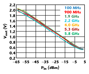 | ||
| Fig. 2 The transfer function of the AD8318 at various frequencies. | ||
Temperature Stability
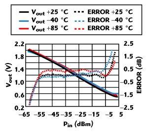
Figure 3 again shows the transfer function of the AD8318 at 5.8 GHz but includes plots of the transfer function at –40° and +85°C. To more closely examine the performance over temperature, the average slope and intercept of the 25°C data is calculated over the most linear part of the curve (–10 to –50 dBm). This yields the familiar straight-line equation for the ideal output voltage for a particular input power
VOUT (mV) = SLOPE(mV/dB)
x (PIN(dBm) – INTERCEPT(dBm))
Next, all three Vout vs. Pin plots are compared with this calculated function. This yields three error plots scaled in dB. Note that the calculated ideal output voltage at 25°C is used as the single reference for all error calculations (including the error at 25°C). This is analogous to the technique that would most likely be used to calibrate the detector in a mass production environment.
 | ||
| Fig. 3 The AD8318 log amplifier’s transfer function vs. temperature at 5.8 GHz. | ||
As one would expect, the error plot at 25°C straddles the 0 dB line. Over temperature, the hot and cold error plots remain well within the ±0.5 dB range for input powers from –6 to –56 dBm.
Response Time
As mentioned earlier, as part of the progressive compression technique that is used in the AD8318, the signals from a series of full-wave detectors are summed and low pass filtered to yield an output voltage that is proportional to the log of the RF input signal. The corner frequency of this low pass filter largely determines the envelope response time (often referred to as the video bandwidth) of the detector.
A fast envelope response time is useful in a number of applications. In many radar and amplitude shift keying (ASK) demodulation applications, the log amplifier is called upon to detect the signal strength and position in time of very short RF bursts. Clearly, the detector must be capable of producing a response to the burst before it starts to decay.
Figure 4 shows the response of the AD8318 to a short 100 MHz burst (at higher frequencies, the envelope response time will be similar). The response shows an attack time (10 to 90 percent of final value) of 11.4 ns and a decay time of 13.2 ns. In practice, the envelope response time of the AD8318 is a little bit faster than this because the envelope of the RF burst is slightly tapered. Note the ripple in the envelope response. This ripple, which is at twice the input frequency, appears because the input frequency and the video bandwidth are close to one another. Additional filtering will remove this ripple but will also slow down the envelope response time.
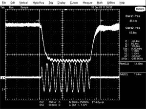 | ||
| Fig. 4 The response of the AD8318 log amplifier to a short 100 MHz burst. | ||