
Industry analyst firm Databeans forecasts the data converter market to more than double between 2011 and 2015, with the high-speed analog-to-digital converter (ADC) and digital-to-analog converter (DAC) markets outpacing all other data converter product categories. Between 2011 and 2015, the firm expects the high-speed ADC market to grow more than 70 percent and the high-speed DAC market to grow about 60 percent.
What’s driving this growth? Just think about how much technology is packed into a new car today versus ten years ago or the increasing number of consumer electronics that most of us depend on – from computers, tablets and e-readers to smartphones, cameras and MP3 players – many of which connect to the global communications network. As technology continues to advance, so too does the need to convert digital signals into the analog world in which we live. And while Databeans forecasts continued growth across all data converter market segments, the firm expects the communications market to grow the most.
To support the needs of communications, defense and aerospace manufacturers, Texas Instruments continues to develop data converters that are faster, smaller and lower power, while also providing higher resolution, ACPR and dynamic range performance. TI’s new quad, 16-bit DACs and direct RF sampling ADCs are examples of how the company is pushing the limits of data conversion to enable its customers to innovate.
DAC3484 series
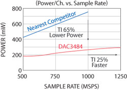
Figure 1 1.25 GSPS, 16-bit DAC reduces power consumption and increases speed.
The 1.5 giga-samples per second (GSPS) DAC34SH84 and 1.25 GSPS DAC3484 are four- channel, 16-bit DACs combining low power consumption, high dynamic range and small size, enabling manufacturers of 3G, LTE and WiMAX base stations, repeaters and software defined radios (SDR) to push the limits of bandwidth and performance while keeping power consumption in check. A wider-input bus DAC34H84 or two-channel DAC3482 are also available to support transmit solutions with DPD linearization bandwidth up to 500 MHz.
The sample rate of the DAC34SH84 clocks in at 1.5 GSPS with a 750 MSPS input data rate per converter, enabling cellular providers to transmit wider signal bandwidths while still using adaptive digital pre-distortion loops, up to 125 MHz using fifth order feedback correction techniques. At 1.25 GSPS, the DAC3484 consumes as little as 250 mW per channel – up to 65 percent less than the closest competitor (see Figure 1) – while enabling wideband power amplifier linearization of up to 250 MHz.
The DAC3484 series simplifies the design of complex transmit architectures with 2× to 16× digital interpolation filters providing more than 90 dB of stopband attenuation to simplify data interface and reconstruction filters. Independent complex mixers allow flexible carrier placement, and a high-performance, low-jitter clock multiplier simplifies clocking without sacrificing dynamic range. The DAC3484 series also includes digital quadrature modulator correction (QMC), enabling complete IQ compensation for gain, offset, phase and group delay between channels in traditional direct up-conversion applications with quadrature modulators. Measuring 9 x 9 mm, the DAC3484 and DAC3482 multi-row QFN package is significantly smaller than comparable DACs, enabling compact designs. The higher speed DAC34SH84 ships in a 12 x 12 mm BGA package.
ADS12Dxx00RF family
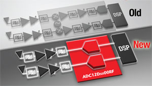
Figure 2 RF sampling ADCs simplify radio design.
The ADS12Dxx00RF family of ADCs is the industry’s first to directly sample RF signals beyond 2.7 GHz, with third-order intermodulation distortion (IMD3) up to -71 dBc and sampling at up to 3.6 GSPS. The family includes five 12-bit ADCs that enable system designers to eliminate multiple intermediate frequency (IF) down-conversion stages, including amplifiers, mixers, LOs and filters, as shown in Figure 2. By replacing entire signal chain subsystems, the ADC12Dxx00RF drastically reduces bill of materials (BOM) cost, board size and weight in 3G/4G wireless base stations as well as microwave backhaul, military and wideband SDR applications.
The ADC12Dxx00RF family provides excellent noise and linearity performance at RF frequencies up to and above 2.7 GHz, extending the usable range beyond the 11th Nyquist zone. The devices provide a flexible LVDS interface with multiple SPI-programmable options for board design and FPGA/ASIC data capture. The LVDS outputs are compatible with IEEE 1596.3-1996 and support programmable common mode voltage.
The ADS12Dxx00RF family includes:
- ADC12D1800RF, providing interleaved single-channel sampling rates up to 3.6 GSPS, or dual-channel rates up to 1.8 GSPS, with IMD3 of -64 dBc at 2.7 GHz.
- ADC12D1600RF, providing interleaved single-channel sampling rates up to 3.2 GSPS, or dual-channel rates up to 1.6 GSPS, with IMD3 of -70 dBc at 2.7 GHz.
- ADC12D1000RF, providing interleaved single-channel sampling rates up to 2.0 GSPS, or dual-channel rates up to 1.0 GSPS, with IMD3 of -69 dBc at 2.7 GHz.
- ADC12D800RF, providing interleaved single-channel sampling rates up to 1.6 GSPS, or dual-channel rates up to 800 MSPS, with IMD3 of -71 dBc at 2.7 GHz.
- ADC12D500RF, providing interleaved single-channel sampling rates up to 1.0 GSPS, or dual-channel rates up to 500 MSPS, with IMD3 of -69 dBc at 2.7 GHz.
Texas Instruments,
Dallas, TX
(972) 644-5580
www.ti.com