
 | |||
The starting point for the design of the S-band high power amplifier was that it had to meet the specifications given in Table 1. These specifications are dictated by the actual operating conditions of the magnetron, which the amplifier is going to feed with microwave power. Solid-state technology is used for the active microwave power devices and the entire design is implemented with microstrips fabricated on Rogers RO4003 substrate with a substrate thickness of 0.51 µm, a copper conductor thickness of 75 mm, a relative dielectric constant of 3.38 and a dielectric loss of 0.0027.
In order to have lower metal resistivity, all the metal conductors are gold plated. The power chain that is suitable to meet the specifications is shown in Figure 1.
All the active devices are from Fujitsu Compound Semiconductors. The first stage is a MMIC, which delivers approximately 33 dB of gain and a 1 dB power output compression point (P1dB) of +41 dBm. The second stage is a power MESFET device with a gain of approximately 11 dB and a P1dB of +43 dBm. The last stage consists of two parallel devices with a gain of approximately 11 dB and P1dB of +51 dBm. The entire coupling networks, which include 90° hybrids, Wilkinson power dividers/combiners and a dual directional coupler, have been customized using microstrip technology. This method keeps the cost low.
 | ||
| Fig. 1 Schematic of the high power S-band amplifier. | ||
At the amplifier output the dual directional coupler is coupled to two RF power detectors that monitor the incident and reflected RF power, then translate them into DC voltages, which can be used for automatic control of the amplifier. For example, if for some reason a high VSWR condition is detected at the output, then the reflected signal and its associated voltage will be too high and an alarm will be activated. Also, forward RF power detection can be used if having an automatic level control (ALC) capability is crucial.
The power supply of the RF amplifier is based on high frequency switching power supply units that deliver constant DC voltages of +10 V, +12 V and –12 V to all the active microwave units separately. Each unit has self-protection circuits to safeguard against over-heating, reverse polarity, and short and open circuits. All power supply units are controlled from a microcontroller in order to set the bias voltages to the correct level at the start-up and shut-off. This is crucial to ensure the long life of the amplifier because the MESFET devices must have a negative bias applied at their gates before the positive drain voltage is applied during the start-up and shut-off sequences. The entire amplifier system is housed in an aluminum box with two high power fans, which hold the temperature of the unit below 40°C during normal operation.
Design Procedure
This amplifier design was a challenging task for many reasons. To begin with, there is a lack of high power GaAs devices operating in the 2.38 GHz frequency range. A significant amount of time was spent finding L/S-band GaAs FETs capable of delivering more than 200 W of microwave power at the center frequency of 2.38 GHz. The amplifying cascade that was finally decided upon was a three-stage chain, as described in the conceptual block diagram of the amplifier.
The first stage uses a FMV5049VT MMIC, the second uses an FLM2527L-20F GaAs FET transistor and the third stage uses a parallel connection of two FLL1200IU-3 push-pull GaAs devices. Two push-pull devices were chosen in order to achieve the desired output power of approximately +53.5 dBm.
The software used for the complete design of the RF chain is Agilent’s ADS2002A. However, since nonlinear models for the three devices were not available in the CAD libraries, the design procedure was based on the use of S-parameters, available on the manufacturer’s Web site. In addition, a list of the optimal Zin and Zout parameters for maximum output power of the push-pull transistors of the third stage was obtained. These parameters were converted into the corresponding input and output reflection coefficients (S11 and S22) of the push-pull device. In order to complete the S-parameter matrix, the forward and reverse transmission coefficients (S21 and S12) from the device datasheet were used.
This technique is not absolutely accurate because the linear gain S-parameters, detailed on the Web site, and the saturated gain S-parameters, obtained in the form of desired matching impedances, are different. However, this provided the opportunity to construct an S-matrix, which makes use of the reflection coefficients and retains information on the transmission behavior of the device. Note that the S-matrix refers to one side of the push-pull device. Given the fact that only S-parameters were available, no nonlinear simulations could be carried out to determine the intermodulation products, the harmonic parasitic effects and the gain compression of the amplifier. The design procedure was based entirely on the information provided by the small signal S-parameters.
Operation Basics
As has been mentioned, the input signal is amplified by the first-stage MMIC device, which then drives the second-stage GaAs FET device. The output signal is then divided into four equal amplitude signals to drive the two push-pull devices. Each of the push-pull states use a balanced configuration design, where the input signals are phase shifted by 90° with respect to each other. The balanced configuration was chosen because it provides better amplifier stability, better matching at the input and output ports, and cancellation of IM3 products and harmonics such as 2F1+F2, 2F2+F1, 3F1, 3F2, etc. The 50 Ω termination at the fourth port of the branch-line coupler improves the amplifier stability and absorbs any reflected signal from the amplifier chain to which it is connected.
The output signal from the second stage was power divided through the use of a microstrip Wilkinson 3 dB coupler. To realize a balanced amplifier design for each push-pull device, a printed microstrip 3 dB branch-line coupler was developed to drive each of the two push-pull devices. The reverse procedure was used at the output for summing the four amplified signals into one.
This power splitting and combining procedure could also be achieved by using commercially available SMT couplers, but a printed version of the couplers was used to keep the costs low. In addition, the frequency bandwidth of the amplifier was only about 5 percent, making it feasible to design and develop near optimum microstrip branch-line and Wilkinson 3 dB couplers.
The internal pre-matching of the MMIC to a 50 Ω system enabled the use of just a 50 Ω microstrip line to apply the input signal to the device. The output of the first stage was matched to the input of the second stage using a microstrip line of the desired characteristic impedance. The output impedance of the second stage was matched to the 50 Ω Wilkinson coupler using a high impedance line. The Wilkinson coupler, designed to divide the signal to the two push-pull devices, uses curved ![]() /4, 70.7 Ω microstrip lines, leaving the gap necessary to place the desired 100 Ω load in-between.
/4, 70.7 Ω microstrip lines, leaving the gap necessary to place the desired 100 Ω load in-between.
The two outputs of the Wilkinson coupler are connected to the branch-line couplers with two 50 Ω microstrip lines of identical length. Each signal is then divided by the branch-line coupler into two parts of nearly the same amplitude and with a 90° phase difference to drive each side of the push-pull transistor amplifier, thus implementing the balanced design.
According to the S-matrix, the input and output impedances of each side of the push-pull device are matched to the 50 Ω branch-line couplers using microstrip lines with different impedances. The output signal from each device is combined again via a branch-line coupler, but received at the opposite port to the one driven at the input. The two combined signals are then summed with a Wilkinson combiner at the output. The branch-line couplers at the input use a 50 Ω, 20 W, RFP-20-50RP high power RF resistor as a terminating load. The couplers at the output utilize a 50 Ω, 40 W, RFP-40-50TR resistor, while the Wilkinson couplers use a 100 Ω, 20 W, RFP-20-100RP resistor. All are Anaren high power RF resistors.
American Technical Ceramics’ 16 pF ATC100A160 DC decoupling capacitors are used in the RF chain. This model offers a very low equivalent series resistance (ESR) and a series resonance at a frequency of 2400 MHz, which is the reason why this value is used in the design.
RF Design Simulation Graphs
Considering the simulated results, Figure 2 shows the linear response of the first-stage MMIC. The gain (S21 parameter) is approximately 31 dB and the return loss both at the input (S11) and output (S22) is well below –18 dB. Also, the Rollette stability factor is well above 1, which means that this is a stable device.
 | ||
| Fig. 2 Linear response of the MMIC first stage. | ||
The Rollette stability factor (K) is given by

where
∆ = S11S22 – S12S21
The Rolette stability factor denotes unconditional stability when it is well above unity, provided that [∆] < 1. The following circuit simulations show that this, nor any other device of the same design, will cause instabilities, as all matched devices have a K>1.
The device needs no matching. Instead single sections of 50 Ω microstrip lines are connected at its input and output pins. Figure 3 shows the linear response of the second stage of the RF chain, which is the FLM2527-20F device with microstrip matching.
 | ||
| Fig. 3 Linear response of the second stage. | ||
Here, the biasing and matching circuits are included in the simulation and, as can be seen, the gain exceeds 14 dB at the desired frequency. The return loss at both ports is well below –10 dB and the Rollette factor is also well above 1, which means that this device is also stable over the desired frequency range.
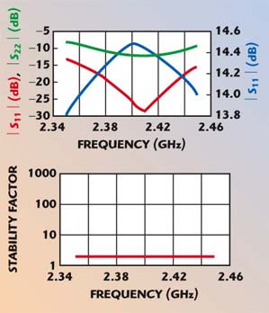
Figure 4 shows the linear response of the FLL1200IU-3 third stage. The simulation includes all the biasing and matching circuits, as well as the microstrip hybrid couplers and the Wilkinson divider/combiners. The overall gain of this final stage is above 13 dB and the return losses are excellent due to the hybrid couplers that are used at both the input and the output. With regard to the return losses, the results are based on true nonlinear RF measurements of the input and output complex impedance of the device, where the S-parameters of the transmission gain are taken into consideration due to the lack of an exclusive nonlinear model of the high power RF device.
 | ||
| Fig. 4 Linear response of the third stage. | ||
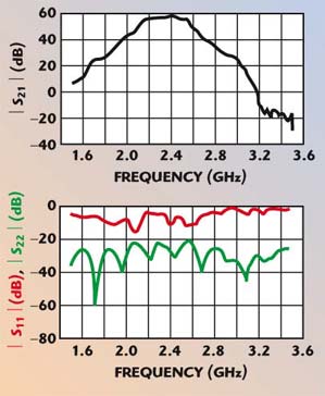
Finally, Figure 5 shows the complete linear response of the entire RF chain. The total linear gain is well above 58 dB and the return losses at both ports are well below –18 dB. The chain exhibits a bandpass behavior due to the matching used between the active devices that makes up the RF chain. Its Rollette factor is also well above 1.
 | ||
| Fig. 5 Linear response of the entire RF chain. | ||
With regards to the simulation of the RF chain, the aluminum housing is taken into account. Its cover is considered to be 15 mm above the microstrip lines in order to prevent possible parasitic oscillations due to electromagnetic coupling from the output to the input of the chain.
Device Bias Circuit Design
The bias circuit design makes use of a ![]() /4 microstrip line with a set of parallel capacitors placed at the end of it, and includes a series resonant capacitor at the fundamental frequency. The
/4 microstrip line with a set of parallel capacitors placed at the end of it, and includes a series resonant capacitor at the fundamental frequency. The ![]() /4 line transforms the capacitors’ low impedance to a very high input impedance circuit, located at the RF chain. An even better way to design an RF biasing circuit is to make use of a quarter-wavelength open circuit stub, also placed at a
/4 line transforms the capacitors’ low impedance to a very high input impedance circuit, located at the RF chain. An even better way to design an RF biasing circuit is to make use of a quarter-wavelength open circuit stub, also placed at a ![]() /4 distance from the origin. This stub presents an input impedance, which is calculated as follows:
/4 distance from the origin. This stub presents an input impedance, which is calculated as follows:
Given that the input impedance of an open-end transmission line, of length l, is
Zoc (l) = –jZ0cotßl (2)
where
![]()
the input impedance of a quarter-wavelength, open circuited line is given by


The quarter-wavelength transform of this stub towards the origin gives an input impedance of infinite value, represented as

However, in this design, an open circuit ![]() /4 line is not used. The reason being that a carefully designed bias stub with a set of capacitors placed at a quarter-wavelength distance from the origin can realize a circuit with very high input impedance for the RF signal, thus providing a simple way to correctly bias the devices with the appropriate currents. Ignoring the
/4 line is not used. The reason being that a carefully designed bias stub with a set of capacitors placed at a quarter-wavelength distance from the origin can realize a circuit with very high input impedance for the RF signal, thus providing a simple way to correctly bias the devices with the appropriate currents. Ignoring the ![]() /4 open circuit stubs also saves space on the amplifier board.
/4 open circuit stubs also saves space on the amplifier board.
For a gate biasing circuit, the ![]() /4 transforming line needs to be one of high characteristic impedance, with the ability to place a small SMT resistor close to the gate to provide GaAs device stabilization. For a drain biasing circuit, the
/4 transforming line needs to be one of high characteristic impedance, with the ability to place a small SMT resistor close to the gate to provide GaAs device stabilization. For a drain biasing circuit, the ![]() /4 line must be of low impedance, due to the high DC drain currents required for the optimum operation of the devices. For this amplifier, the capacitors used at the end of each
/4 line must be of low impedance, due to the high DC drain currents required for the optimum operation of the devices. For this amplifier, the capacitors used at the end of each ![]() /4 biasing line were a 16 pF capacitor resonating at the center frequency and a 100 pF capacitor to filter out lower frequency instabilities.
/4 biasing line were a 16 pF capacitor resonating at the center frequency and a 100 pF capacitor to filter out lower frequency instabilities.
Device DC Supply
For the gate DC supply of each device, an adjustable output voltage circuit was designed and implemented on the amplifier board. These six adjustable output circuits are supplied from a single –12 V, 2 A negative voltage source, which is able to provide all the necessary gate currents. The drains of the two first-stage transistors are supplied from a 10 to 18 V, 20 A adjustable switching power supply. Note that these two devices need the same drain voltage, so the biasing circuits are joined with a low impedance microstrip line. Note also that the MMIC device has two drain DC supply pins, which are joined together after the l/4 bias line. For the drain supplies of the two push-pull devices of the amplifier, four of these power supplies are used, as each side of the device demands approximately 13 A of current at full RF drive. The complete layout of the RF amplifier chain is shown in Figure 6, including all the bias circuitry needed for its optimum operation.
 | ||
| Fig. 6 Layout of the RF amplifier printed circuit board. | ||
Measurement Results
Two 220 VAC fans housed in the aluminum box containing the RF chain provide thermal relief to the base of the RF chain, which is crucial in order to achieve a good MTBF. The RF chain and associated DC power supply circuitry is housed in a wheeled box and the total weight of the system is approximately 50 kg. The system operated continuously for several hours and the output power remained constant within ±0.25 dB at its maximum rating. Figure 7 shows the set up used to measure the small signal performance of the system.
 | ||
| Fig. 7 S-parameter measurement system. | ||
As can be seen, a high power directional coupler, together with a high power 50 Ω termination and a 30 dB additional attenuator, are used to prevent accidental damage to the vector network analyzer. A 220 VAC/5 A power supply unit supplies the whole system with the desired sequence, which means that the negative voltages are applied at the gates first and then the positive voltages at the drains. The sequence is reversed for the shut down procedure.
The output power is coupled to a 30 dB attenuator through the use of a high power directional coupler. All the intermediate losses from input to output are taken into account during the vector network analyzer calibration procedure. The first testing of the system resulted in the performance shown in Figure 8.
 | ||
| Fig. 8 First testing of the power amplifier. | ||
As shown, the return loss at the output is excellent, mainly due to the hybrid couplers used, whereas at the input it is evident that additional matching is needed. However, the measured gain is just 1 dB less than the predicted simulated value. The system is then matched at the input with an open stub 3 mm long and 2 mm wide. The results are given in Figure 9.
 | ||
| Fig. 9 Measured results after retuning the amplifier input. | ||
The results show that a slight change in gain is observed which has no great significance although there is great improvement in the input return loss, together with a slight improvement in the output return loss. The position of the stub is decided empirically based on real time measurements with the vector network analyzer.
A comparison of the measured and simulated S-parameters is given in Figure 10. Good agreement is observed, especially at the center design frequency of 2.38 GHz. With regard to the output return loss, the graphical difference shown is of minor interest since the absolute mean value is below –25 dB. Therefore, any differences in the region of ±3 dB are not significant. The input return loss correlates well with the simulated results, where the gain (which is the most crucial index) exhibits good agreement for a bandwidth of about 100 MHz around the center frequency of 2.38 GHz.
 | ||
| Fig. 10 Comparison of measured and simulated S-parameters of the amplifier. | ||
Appendix A shows the nonlinear measurement set up. A synthesized microwave signal feeds the amplifier with swept power and a microwave power meter and spectrum analyzer measure the absolute power and the harmonics, respectively.
First, the swept power is delivered at three different frequencies within the pass-band in order to check the flatness of the amplifier at its maximum output power capability. Figure 11 shows the results for the three frequencies’ output power level.
 | ||
| Fig. 11 Pout vs. Pin for three different frequencies. | ||
On the same plot there is also the ideal linear gain response (with no compression) as a comparison with the real values of output power. As shown, the output power at the 1 dB compression point at 2.38 GHz is approximately +53 dBm. In Figure 12 the level of the higher order harmonics is shown versus the sweeping input power of the 2.38 GHz fundamental frequency. It can be seen that the level of the higher order harmonics is well below 50 dBc compared to the fundamental even at the saturation level of the amplifier.
 | ||
| Fig. 12 Measured output power of higher harmonics vs. input power at the fundamental frequency. | ||
Figure 13 shows the power level of the third, fifth and seventh intermodulation products versus the input power level of each of the tones at 2.380 and 2.381 GHz. From this figure, the IP3-out is approximately +57 dBm.
 | ||
| Fig. 13 Intermodulation product levels. | ||
Conclusion
The design of a high power S-band solid-state power amplifier has been presented. It will be used as a driver amplifier for the electron beam pre-acceleration and chopping cavities of the linear accelerator based in the Institute of Accelerating Systems and Applications of the University of Athens. The challenge was to find high power GaAs FETs that are capable of delivering the proper amount of RF power at the center frequency of 2.38 GHz. Simulation and measurement results are presented, and good agreement is observed despite the fact that no nonlinear models of the active devices were available.
References
- G. Gonzalez, Microwave Transistor Amplifiers: Analysis and Design, Second Edition, Prentice-Hall Inc., Upper Saddle River, NJ, 1997.
- P.L.D. Abrie, Design of RF and Microwave Amplifiers and Oscillators, Artech House Inc., Norwood, MA, 1999.
- J. Shumaker, R. Basset and A. Skuratof, “High Power GaAs FET Amplifiers: Push-pull versus Balanced Configurations,” Wireless Symposium 2001, San Jose, CA, www.fcsi.fujitsu.com.
- N.K. Uzunoglu, Introduction to Microwaves, Second Edition, Papasotiriou Inc., 1994.
- Datasheets, FMM5049VT, FLM2527L-20F and FLL1200IU, www.fcsi.fujitsu.com.