
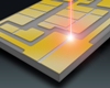
 Solder flows. Ideally, it flows where needed, but molten solder tends to have a mind of its own. To prevent unwanted flow, many PCB designers will install dams formed of glass or other dielectric materials to keep solder from shorting active areas on a circuit. But there is another solder damming technique being rapidly adopted—laser ablation. Considered to be more accurate and consistent than traditional solder damming methods, laser ablation vastly improves the production process by increasing repeatability and significantly reducing manufacturing costs. Whereas traditional methods of printing and firing glass or other dielectric masks can be costly in terms of processing time, labor, and scrap material, “laser trenches” around a solder pad can be made simply and they are inherently more repeatable. Conventional glass or dielectric print and fire processes are also limiting in terms of resolution, and create structured solder dams with typical widths of 0.030 in. In contrast to these techniques, laser trenches provide better resolution and take up considerably less space on a PCB by forming solder dams with typical widths of just 0.007 in.
Laser Control
Each type of laser system has a specific optical wavelength, such as 1064 nm for a Nd:YAG laser and about 10,640 nm for a CO2 laser. Laser ablation can deliver reliable and consistent solder dams with widths as fine as 0.006 in., with accuracy and repeatability of typically ± .0015 in. When the proper setup is achieved, exacting amounts of power remove only the layers of top material (typically Au/Ni) needed, exposing the mid-layers that form the trench without exposing sensitive base materials. Laser Services can also control the laser to ablate through and over edges of the PCB, again without impacting important base materials.
The Added Value of Laser Ablation
Laser Services’ laser machining systems are compatible with standard computer-aided-manufacturing (CAM) and computer-aided-design (CAD) circuit artwork files. The fast processing speeds of these computer-controlled systems translate to fast PCB turnaround times and low production costs.
Laser ablation is also useful for a variety of other tasks, including repairing PCBs by removing conductive traces without damaging surrounding areas. It can also be used for machining dielectric and copper materials to form unique surface features such as chamfers around cutouts. The fine resolution of lasers also delivers high isolation even on densely populated PCBs. For small-piece orders or large production runs, laser ablation provides the utmost flexibility and processing speeds for a wide range of PCB manufacturing applications. Laser ablation is incredibly accurate and forms solder dams with less material and less labor than any other PCB solder damming process. Consider laser ablation the next time you’re looking to control solder flow and production costs.
![]()