
Mobile telecommunication devices continue to add functionality and complexity particularly in regards to the trend of integrating more wireless bands such as GSM, E-GSM, CDMA, W-CDMA, DCS and PCS. This trend has increased the complexity of the transmit/receive and diversity antenna switch components resulting in a migration away from PIN diodes to multi-gate pHEMT devices. The performance advantages of multi-gate pHEMTs compared to PIN diode switch components include lower insertion loss, lower power consumption (since diode switch components require continuous applied bias for switching operation) and reduced size (as a MMIC pHEMT replaces multiple PIN diode devices in multi-band switches).
A technology development program was initiated to develop D-mode pHEMT switch components to respond to the perceived trends in the mobile telecommunications module market. The technology development leveraged pHEMT expertise, development and production on 100 mm substrates and high density, low dielectric constant interconnect architecture on 150 mm substrates1 plus a combined effort from design, modeling, epitaxy engineering and process development on careful optimization of all areas through detailed cross-correlation to final product characteristics. The GSM switch components were optimized to create industry-leading insertion loss and harmonic suppression characteristics, while the CDMA switch components were optimized to create industry-leading insertion loss and cross-modulation suppression characteristics. To reduce the number of control lines in multi-band modules and switch components, decoders are being incorporated. The D-mode pHEMT switch components satisfy user needs for power amplifier modules since decoder logic is typically incorporated into the CMOS chip along with power control functions for the power amplifier. The situation is different for an antenna switch module wherein user feedback suggests that the decoder functions must be incorporated with the switch component. The integration of E- and D-mode transistors to enable digital logic decoding functions was explored to reduce the control line count in antenna switch modules.
A variety of approaches have been applied in literature2–4 to integrate E- and D-mode HEMTs for assorted applications as well as switch plus decoder logic applications.5–7 An E-mode device development approach was chosen to not only provide the ability to perform digital functions but also to enable pHEMT-based power amplifier performance that provides an alternative to GaAs heterojunction bipolar transistors in mobile telecommunications. A few points of attraction of an E-mode pHEMT process for cellular power amplifier applications include no thermal runaway, softer breakdown characteristics and good survivability under large mismatch conditions, high transconductance at low quiescent current enabling class B or sub-class B operation,8 low voltage operation due to low turn-on voltage, and the absence of large voltage drops due to p-n junctions, as well as potential integration with switch, passive and low noise amplifier components. This robust and multi-function E-/D-mode pHEMT process named TQPED is leveraging off of TriQuint foundry’s success and wide spread use of the E-/D-mode MESFET process with the moniker TQTRX. Detailed load-pull investigations under different modulation formats were performed and cross-correlated to epitaxy engineering, transistor architecture and integration techniques for the E-mode transistor, while preserving D-mode switch component performance. A summary of select load-pull performance characteristics will be presented.
Device and Process Technology
The process utilizes molecular beam epitaxy (MBE) grown material on a variety of different types of 150 mm GaAs substrates. The structure of the epitaxy consists of a thin, undoped, pseudomorphic InGaAs channel layer surrounded on both sides by delta-doping layers that provide carriers to the channel. Undoped AlGaAs spacer layers are grown in between the channel and the delta-doping layers. A Schottky layer of AlGaAs is placed on top of the upper spacer layer to target the desired pinch-off voltage, forward voltage and transconductance. InGaP is used as a highly selective etch stop layer and N+ GaAs is used for the ohmic contact layers. Typical room temperature Hall measurements produce sheet carrier concentrations of 3.15E12 cm–2 and electron low field mobility in excess of 6500 cm2/V•s. A double recess technique is used for both the D- and E-mode devices to produce high breakdown voltage. This recess also enables the formation of N-epitaxy resistors that possess a nominal sheet resistance of 285 Ω/sq. Precision NiCr resistors with a sheet resistance of 50 ±3 Ω/sq and approximately zero temperature co-efficient are also available. Local interconnects are used as device contacts to the transistors, varactors, resistors and Schottky diodes. This metal is also used as the bottom plate of a high precision metal-insulator-metal (MIM) capacitor. The MIM has a capacitance per unit area of 0.63 ± 0.10 fF/μm2 and a maximum voltage rating of 40 V. The interconnect architecture utilizes a planarizing, interlevel dielectric composed of benzocyclobutene (BCB) with relative permittivity of 2.7. A representative scanning transmission electron microscopy cross-section of the process architecture is displayed in Figure 1.
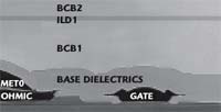 | ||
| Fig. 1 STEM cross-section of the pHEMT process. | ||
The excellent degree of planarization of the BCB can clearly be seen over the gate, ohmic and Metal0 features. The nominal thickness of Metal1 and Metal2 are 2.0 and 4.0 μ m, respectively. The first layer of BCB is nominally 1.0 μ m thick; the second layer is 2.8 μm thick.
The D-mode transistor pinch-off voltage is centered at –800 mV with a process window of ± 200 mV. The nominal IDSS (Vgs = 0 V) corresponding to the centered pinch-off voltage is 200 mA/mm, while the nominal IMAX (Vgs = +1 V) is 500 mA/mm. The on-resistance at IMAX is 1.5 Ω • mm and the typical drain-gate breakdown voltage is 17 V. The Ids to Vds relationship of a typical D-mode transistor is presented in Figure 2. The circles represent measured data, while the solid lines are the modeled characteristics. The models are based on the charge control TOM3 implementation.
 | ||
| Fig. 2 Ids vs. Vds characteristics of a typical D-mode transistor. | ||
The E-mode transistor pinch-off voltage is centered at +350 mV with a process window of ±150 mV. The nominal IMAX is 290 mA/mm and the nominal IDSS is 0.0005 mA/mm. The on-resistance at IMAX is 2.5 Ω • mm. The Ids to Vds relationship of a typical E-mode transistor is presented in Figure 3.
 | ||
| Fig. 3 Ids vs. Vds characteristics of a typical E-mode transistor. | ||
The subthreshold characteristics of the E- and D-mode devices are nominally 75 and 95 mV/decade, respectively. The very steep subthreshold characteristics of the E-mode device enable the transistor to be fully shut off when zero voltage is applied across the gate-to-source junction. The subthreshold curves of both the E- and D-mode transistors are presented in Figure 4. Both the E- and D- mode transistors exhibit in excess of 6 orders of magnitude drain-to-source current swing from deep subthreshold to IMAX bias points.
 | ||
| Fig. 4 Subthreshold characteristics of E- and D-mode transistors. | ||
The transconductance (Gm) as a function of Vgs variation was optimized to have a relatively large region of constant, peak value.9 The transconductance has a good plateau in peak value over a wide range of Vgs values and does not exhibit any spurious inflection points or additional peaks, as can be seen in the extrinsic transconductance to Vgs relationship shown in Figure 5.
 | ||
| Fig. 5 Gm and Ids vs. Vgs. | ||
A minimum D-mode pHEMT drain-to-gate breakdown voltage of 15 V was required for 1 μA/μm current levels but, to maintain such a breakdown voltage with excellent process latitude, a trade off with on-resistance, output power and gain was made.10 A similar trade off was made for the E-mode pHEMT device. This results in two separate processes — one optimized for switch performance and the other for power amplifier performance.
The performance of the TQTRX MESFET process is contrasted against the TQPED pHEMT technology in Table 1. The MESFET process offers two D-mode transistors with differing pinch-off voltage. The device with a more negative voltage is called the G-mode device and is more suited for power applications. The pHEMT devices produce substantially more available current for a given pinch-off voltage relative to the MESFET devices and with much better transconductance and subthreshold characteristics. In addition, the E-mode pHEMT is a true E-mode device that is fully pinched-off over process variation and temperature. Typical temperature dependence of the pinch-off voltage is –1 mV/°C. The D-mode pHEMT ft is 27 GHz at Vds = 3.0 V and at Idss/2 with fmax in the 90 GHz range producing a good fmax to ft ratio. Maximum stable gain is approximately 22.5 dB at 2 GHz and the Gm to Gds ratio is 40. The E-mode pHEMT ft is approximately 30 GHz at Vds = 3.0 V and at Vgs = 0.9 V with fmax in the 100 GHz range. Very high maximum stable gain is achieved, approximately 27 dB at 2 GHz. Additionally, an excellent Gm to Gds ratio of 110 is realized at Vds = 3.0 V and Vgs = 0.9 V.
 | ||
The noise performance of both pHEMT devices was analyzed over different bias points and frequency ranges. The results at Vds = 3.0 V are presented in Figure 6. The D-mode is biased at IDSS/4 = 50 mA/mm, whereas the E-mode is biased at IMAX/4 = 64 mA/mm. The large difference in gain between the D- and E-mode device is also evident in this figure.
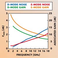 | ||
| Fig. 6 Noise figure and associated gain. | ||
Large-signal Characteristics
Detailed load-pull measurements were performed on both the D- and E-mode pHEMTs to determine the power performance, optimum source and load tuning conditions, optimum bias conditions and estimates of quiescent current, all as a function of the different modulation formats which include continuous-wave, CDMA IS95A and EDGE. These evaluations were performed across epitaxy variants, transistor geometry and process modifications to determine the optimum structures for linearity and saturated power performance.
The D-mode pHEMTs were measured under continuous-wave formats at 1.9 GHz with a bias of Vds = 8.0 V and Ids = IDSS/2. Peak values of gain, power-added efficiency (PAE) and output power (Pout) were determined to be 29 dB, 64 percent and 530 mW/mm, respectively. Excellent operation was obtained up to Vds = 17 V and IDSS/2 with output power increasing to beyond 1200 mW/mm, as shown in Figure 7.
 | ||
| Fig. 7 Load-pull data of a D-mode pHEMT at 1.9 GHz. | ||
The load-pull characteristics of the E-mode pHEMTs were examined under continuous-wave, CDMA and EDGE-GSM modulation formats, all at 1.9 GHz with a Vds = 3.5 V (see Figure 8). The saturated characteristics of the E-mode indicate that excellent PAE of 81 percent and Pout of 245 mW/mm are achievable at the 3 dB gain compression point, which in this case was 19 dB. Quiescent current was 12 mA/mm.
 | ||
| Fig. 8 Load-pull data of an E-mode pHEMT at 1.9 GHz. | ||
Optimum performance of the E-mode device under CDMA IS95A modulation required tuning of the second harmonic termination as well as the fundamental. Very good adjacent channel efficiency is obtained at –50 dBc adjacent channel power ratio (ACPR), as shown in Figure 9. Adjacent channel Pout and gain were 120 mW/mm and 17.5 dB, respectively. Quiescent current was 8 mA/mm.
 | ||
| Fig. 9 Load-pull data of an E-mode device under CDMA IS95A conditions. | ||
Performance under EDGE-GSM modulation was also analyzed. The ACPR specifications included –35 dBc at 200 kHz, –60 dBc at 400 kHz and –70 dBc at 600 kHz. The limiting specification in virtually all cases was the 400 kHz ACPR. The load tuning conditions for EDGE and GSM modulation are not too different and therefore an excellent compromise can be reached. The simultaneous optimization of EDGE and GSM required the input power for EDGE to be backed off by 3.5 dB relative to GSM modulation. Under GSM modulation the PAE, gain and Pout was 73 percent, 18.7 dB and 215 mW/mm, respectively. Under EDGE modulation the adjacent channel PAE, gain and Pout was 52 percent, 19.1 dB and 108 mW/mm, respectively.
Product Applications
A SP4T GSM switch with built-in decoder function and electrostatic discharge protection was created and measured. The small-signal performances of the switch transmit and receive paths are shown in Figure 10 with four traces for each of the transmit to receive. The insertion loss and harmonic generation at a control voltage of 2.7 V for 836.5 and 1880 MHz is displayed in Figure 11. The circuit has excellent insertion loss of approximately 0.45 and 0.55 dB at low and high band, respectively. At 34.5 dBm and low band, the second and third harmonic generation is approximately –75 dBc, while at 32 dBm and high band, the second and third harmonic generation is approximately –78 dBc.
 | ||
| Fig. 10 Insertion loss and return loss of a GSM SP4T switch for the (a) transmit and (b) receive paths, and transmit-to-receive isolation. | ||
 | ||
| Fig. 11 Insertion loss plus second and third harmonic generation vs. input power at (a) 836.5 and (b) 1880 MHz. | ||
The decoder current dissipation as a function of input power at 2.7 V control voltage is presented in Figure 12. The decoder current at both high and low band is virtually identical. At Pin of 32.5 dBm the decoder current is only 160 μA; at 34.5 dBm it increases to only 170 μA.
 | ||
| Fig. 12 Decoder current consumption as a function of input power. | ||
Harmonic generation of the SP4T switch versus external transmit filter match at the harmonic frequencies is shown in Figure 13. The fundamental termination in band is 50 Ω and the VSWR for harmonic frequencies are 8 (low band) and 5 (high band), respectively. In each band, the second and third harmonic performances are independent of each other’s phase (phase at the second harmonic does not affect the third harmonic performance and vice versa). Low band conditions were Pin = 35 dBm at a frequency of 836.5 MHz, with a Vdd = 2.7 V. High band conditions were Pin = 33 dBm at a frequency of 1880 MHz and Vdd = 2.7 V.
 | ||
| Fig. 13 Second and third harmonic generation as a function of the phase at (a) low band with an 8:1 termination VSWR and (b) high band with a 5:1 termination VSWR. | ||
Conclusion
A detailed and thorough presentation of a newly developed 0.5-μm gate length E-/D-mode pHEMT process on 150 mm substrates with BCB-based interconnects was presented and discussed. The E- and D-mode transistors exhibit large IMAX values with excellent subthreshold, breakdown, ft, fmax, Gm/Gds and transconductance characteristics. Load-pull results have been presented under a variety of modulation formats with good PAE performance combined with impressive linearity, output power and gain. A GSM SP4T switch with built-in logic decoder and electrostatic discharge protection was designed, built and tested. Excellent small-signal and large-signal performances were achieved. Small-signal transmit and receive path losses were 0.50 to 0.60 dB and 0.55 to 0.65 dB, respectively. Switch transmit-to-receive isolations were better than 32 dB. Large-signal harmonics in the presence of transmit filter harmonic mismatch were better than –69 dBc (low band) and –70 dBc (high band), respectively. Quiescent DC decoder current draw was less than 170 μA from a 2.7 V supply.
References
- E.P. Finchem, W. Mickanin and C. Rosemeyer, “A Multi-level High Density Interconnect Process Designed and Developed for Manufacturability,” GaAs MANTECH, April 1994, pp. 163–166.
- A. Mahajan, P. Fay, M. Arafa, G. Cueva and I. Adesisa, “Monolithic Integration of InAlAs/InGaAs/InP Enhancement- and Depletion-mode High Electron Mobility Transistors,” IEDM, December 1996, pp. 51–54.
- M. Tong, K. Nummila, J.W. Seo, A. Ketterson and I. Adesida, “Process for Enhancement-/Depletion-mode GaAs/InGaAs/AlGaAs Pseudomorphic MODFET’s Using Selective Wet Gate Recessing,” Electronics Letters, Vol. 28, 1992, pp. 1633–1634.
- T. Suemitsu, H. Yokoyama, Y. Umeda, T. Enoki and Y. Ishii, “High Performance 0.1-mm Gate Enhancement-mode InAlAs/InGaAs HEMT’s Using Two-step Recess Gate Technology,” IEEE Transactions on Electron Devices, Vol. 46, No. 6, June 1999, pp. 1074–1079.
- S. Kusunoki, T. Ohgihara, M. Wada and Y. Murakami, “SPDT Switch MMIC Using E-/D-mode GaAs JFETs for Personal Communications,” GaAs IC Symposium, November 1992, pp. 135–138.
- H. Tosaka, T. Fujii, K. Miyakoshi, K. Ikenaka and M. Takahashi, “An Antenna Switch MMIC Using E-/D-mode pHEMT for GSM/DCS/PCS/WCDMA Bands Application,” RFIC Symposium, June 2003, pp. 519–522.
- D.W. Wu, R. Parkhurst, S.L. Fu, J. Wei, C.Y. Su, S.S. Chang, D. Moy, W. Fields, P. Chye and R. Levitsky, “A 2W, 65% PAE Single-supply Enhancement-mode Power pHEMT for 3 V PCS Applications,” IEEE International Microwave Symposium, June 1997, pp. 1319–1322.
- Y.A. Tkachenko, Y. Zhao, C. Wei and D. Bartle, “Enhancement-/Depletion-mode InGaP/AlGaAs pHEMT for High Efficiency Power Amplifiers,” Microwave Journal, Vol. 44, No. 4, April 2001, pp. 122–128.
- Y.A. Tkachenko, D. Bartle, and C.J. Wei, “Correlation Between Ungated Recess Width and Linearity of GaAs MESFETs,” Microwave Journal, Vol. 42, No. 7, July 1999.
- K. Higuchi, H. Matsumoto, T. Mishima and T. Nakamura, “Optimum Design and Fabrication of InAlAs/InGaAs HEMT’s on GaAs with Both High Breakdown Voltage and High Maximum Frequency of Oscillation,” IEEE Transactions on Electron Devices, Vol. 46, No. 7, July 1999, pp. 1312–1317.