
Radio-frequency (RF) circuit design has become more complicated as today’s products and technologies have evolved, while at the same time the required design cycle times have been reduced. This presents problems for designers using traditional RF and microwave design techniques, which utilize similar procedures whether done with simulation software or on a test bench in the laboratory. Typically, these traditional methods involve designing and simulating/ testing the individual sections of a design (such as matching networks, gain stages and bias circuits), assembling the pieces together, evaluating the overall performance and tweaking until the design specifications are met. The potential area of “disconnect” in this design method is that the individual sections are usually designed and simulated using 50 Ω input and output terminations to emulate network analyzer testing. However, the actual circuit sections are not terminated in an ideal 50 Ω, they are terminated by the impedance of the adjacent stages. These stages present a load that is not only complex, but is also frequency-variant.
Fortunately, electronic design automation (EDA) vendors have recently introduced new platforms that address these challenges in a completely different way, opening the door to future progress in streamlining the RF circuit development process. New architectures are now available for faster and more accurate design of the individual sections of an amplifier in the context of the actual assembled circuit, not just as in a stand-alone 50 Ω system. The importance of this approach is illustrated by looking at the example provided in this article, which discusses techniques to understand the actual “in circuit” gain, loss and matching characteristics of each section of the overall circuit. As a result, the assembly and tuning of the entire design is done in conjunction with the design of the individual sections. Furthermore, designers gain unprecedented insight into the operation of their circuit and all of its interdependencies, which ultimately leads to faster design cycles, a higher first-pass success rate and higher yields.
Two-stage Amplifier Example
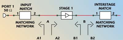
The example circuit is a typical two-stage amplifier shown in Figure 1. The design can be divided into five discrete sections or sub-circuits:
- input matching network
- first gain stage
- inter-stage matching network
- second gain stage
- output matching network
 | ||
| Fig. 1 Typical two-stage amplifier schematic. | ||
To simplify further discussion, the “nodes” between each of these sections are referred to sequentially as A to D.
Generally, the small signal design concerns for this type of amplifier involve power gain (S21), match (S11 and S22), reverse isolation (S12) and, perhaps, noise figure (NF). To meet all of the design criteria, the passive matching stages must properly do their job as impedance transformers. That is, they must appear to have a given impedance on their input node, and then transform it such that they appear to have another impedance on their output node. A good example can be seen by looking at the input matching network. Its job is to transform the system impedance on its input side to another impedance on its output side (node A). Similarly, the inter-stage match should transform the impedance at node B to the impedance at node C, and the output match should transform the impedance at node D to the system impedance.
The impedance transformation task is slightly more complicated in that there are actually two impedances at every labeled node. These are the impedance looking to the left of the node and the impedance looking to the right of the node. Again, to simplify further discussion, these impedances are labeled “sub-node 1” and “sub-node 2,” where sub-node 1 always looks to the left of a node and sub-node 2 always looks to the right of a node (see Figure 2).
 | ||
| Fig. 2 Schematic showing the two impedances associated with a node. | ||
Although there are many possible design goals, an illustrative case to consider is that of maximum power transfer. In general terms, maximum power transfer occurs when the two impedances at any given node are the complex conjugate of one another. More specific to the example presented, maximum power transfer will occur between the input match and the first gain stage if sub-node A1 is equal to the complex conjugate of sub-node A2. It follows that the same relationship should hold true for the other three nodes in the system. Simplistically speaking, the main problem presented to the designer is determining the impedances at the gain stage sub-nodes like A2 (and B1, C2 and D1), as these directly provide the target numbers for design of the matching networks.
A classical design approach to solving this impedance problem is to characterize the gain stages in a 50 Ω environment (see Figure 3). This involves measuring every stage on a test board in the lab, or simulating each stage as if it were connected to a network analyzer (and perhaps a noise figure meter). The resulting S-parameter data (and impedance information) can be plotted on a Smith chart. An S11 simulation of only the first gain stage provides the A2 numbers (just as S22 provides the B1 numbers). Given these numerical targets, the matching networks are designed, the amplifier sections are cascaded together and the overall circuit is tweaked for optimal performance.
 | ||
| Fig. 3 Characterization of gain stage impedances in a 50 Ω environment. | ||
The potential problem with this approach is that the analysis of each gain stage is performed in a 50 Ω system. The real gain stages, however, are not in a 50 Ω system when they are inserted into the complete amplifier design. Instead, they are surrounded by circuits that present a complex, frequency-dependant load impedance. The real loading conditions, coupled with the fact that active devices are not unilateral (S12 ≠ 0), means that, within the actual circuit, the sub-node impedances are different from those calculated in a 50 Ω system. For example, consider the sub-node A2 impedance. As it changes, the target impedance for the input matching network design also changes. The result is that the actual circuit loading conditions move the maximum power transfer point away from the 50 W design point causing the node A junction to perform sub-optimally. Figure 4 shows an example of S11 differences between a 50 Ω system and the actual circuit loading conditions (notice the difference in the range of impedances). The blue trace shows the A2 impedance when simulated into 50 Ω, while the red trace shows the impedance when the first gain stage is terminated with the actual circuit loading conditions.
 | ||
| Fig. 4 Node A2 impedance with 50 Ω and actual circuit loading. | ||
To properly design the matching networks for the correct circuit impedance, a different design methodology is required that can simultaneously consider the actual circuit impedances at every node in the design and allow the designer to quickly understand and move towards a global solution.
A review of the amplifier schematic shows that the sub-node A2’s actual impedance is realized by looking into the first gain stage, the inter-stage matching network, the second gain stage, the output matching network, and, lastly, 50 Ω. Thus, proper characterization of A2 requires an S11 simulation of the network shown on the right in Figure 5. It is important to realize that there are multiple circuit sections in this A2 impedance simulation. This means that changes to any of these sections (first gain stage, inter-stage matching network, second gain stage, or output matching network) will affect the A2 impedance. Similar to the A2 impedance measurement, sub-node A1’s impedance can be monitored by looking back though the input matching network and then 50 Ω, requiring an S22 simulation of the network on the left. A Smith chart plot of impedance at sub-node A1 and the conjugate of the impedance at sub-node A2 will show the two curves converging as the matching network design approaches the ideal power transfer impedance.
 | ||
| Fig. 5 Proper characterization of the A2 impedance. | ||
A closer look reveals that the sub-node A1 and A2 impedance simulations are accomplished by breaking the node connection and treating each individual side of the node as an independent two-port network terminated with 50 Ω. This same splitting technique can be used to characterize the remaining sub-nodes in the circuit (B, C and D). By creating all of the appropriate two-port networks, a designer has accurate and complete knowledge of the actual circuit load impedances on each terminal of the gain stages, which, in turn, leads to accurate target impedances for the matching network designs. Monitoring all of the sub-nodes in this fashion opens up the “black box” designers often face in a traditional design approach. This provides an opportunity to ensure that each node is optimally matched for the design constraints, which ultimately leads to designs that are better centered, have higher performance and higher yields.
Additional complexity exists in that real matching networks are much more than simple transformers. They have a finite bandwidth and insertion loss, which, like the sub-node impedances, are most appropriately analyzed with the actual circuit impedances. Both of these figures of merit can have a big impact on overall design success, as the finite bandwidth can lead to roll-off problems and extra insertion loss reduces output power and raises the noise floor. Figure 6 shows an example of S21 differences between a 50 Ω system and actual circuit loading conditions of a matching network (note the significant difference in the matching network bandwidth and insertion loss).
 | ||
| Fig. 6 Insertion loss of a matching circuit for different matching conditions. | ||
Fortunately, by setting up the impedance simulations mentioned above and using the concept of “network terminations,” the real insertion performance characteristics are available. As an example, consider the inter-stage matching network in the two-stage amplifier. Reviewing the schematic again shows that on the input side, it is terminated by looking back through the first gain stage, the input matching network, and then 50 Ω. On the output side, it is terminated by the second gain stage, the output matching network, and, lastly, 50 Ω. Both of these terminations are complex and frequency-dependant, which is not something that can be measured in the laboratory with traditional 50 Ω network analysis equipment.
Network terminations are a simulation aid that allows one network to be terminated with the impedance of another network. This simulation set up is straightforward, as the necessary circuit fragments for proper termination are already created during the sub-node impedance simulation. In particular, terminating the left side of the inter-stage matching network with the sub-node B1 impedance simulation and terminating the right side with the sub-node C2 impedance simulation will provide the actual circuit performance (see Figure 7).
 | ||
| Fig. 7 Using network terminations in the circuit simulation will provide overall circuit performance. | ||
The network termination concept can be expanded to the gain stages as well as the passive networks, enabling active device performance evaluation in the context of the actual circuit. Combining all of the insertion simulations, sub-node impedance simulations and front-to-back simulations is the key to this design methodology (see Figure 8). The result is a single simulation set up in which every aspect of a circuit’s performance can be accurately explored. The simulation set up effort required by this method is not much greater than with the traditional design approach, especially where proper hierarchy is used for each of the network sections (as shown in the examples). In the very early stages of the design, dummy circuits or behavioral models can be used for the matching networks so that, as the designs develop, the desired information is readily available. For a two-stage amplifier design, the complete procedure involves from 10 to 15 two-port simulations. Recent advances in simulation architecture make it possible to simulate rapidly enough to allow real time tuning of component parameters while monitoring the intermediate matching conditions, actual sub-circuit performance and overall response. Additionally, measurement driven software makes it easier than ever to perform optimization or yield sensitivity analysis with goals coming from any of the 10 to 15 two-port networks.
 | ||
| Fig. 8 Combining insertion simulations, sub-node impedance simulations and front-to-back simulation is the key to the design methodology. | ||
Conclusion
RF and microwave design specifications are more demanding than ever, while design cycle time requirements continue to decrease. The opposing nature of these two demands can put a strain on engineers and their traditional design methodology. Design software can provide a tremendous advantage, especially when it is capable of providing designers with a “virtual” world in which to perform simulations and gain circuit insight that is just not available on a bench in the laboratory. The design methodology explained in this article does exactly that — it removes the constraints of a physical test bench in the laboratory and provides unprecedented insight into any RF and microwave circuit’s performance and operation.
Acknowledgment
The author would like to thank the engineers at Raytheon and TriQuint for sharing their time and knowledge to develop the methodology described in this article.